

Method for reducing full light switch pump power, full light switch and its preparing method
An all-optical switch and pump power technology, applied in optics, nonlinear optics, instruments, etc., can solve problems such as low transmittance, complicated preparation process, and reduced pump light intensity, and achieve easy integration and simple preparation technology , the effect of low pump power
- Summary
- Abstract
- Description
- Claims
- Application Information
AI Technical Summary
Problems solved by technology
Method used
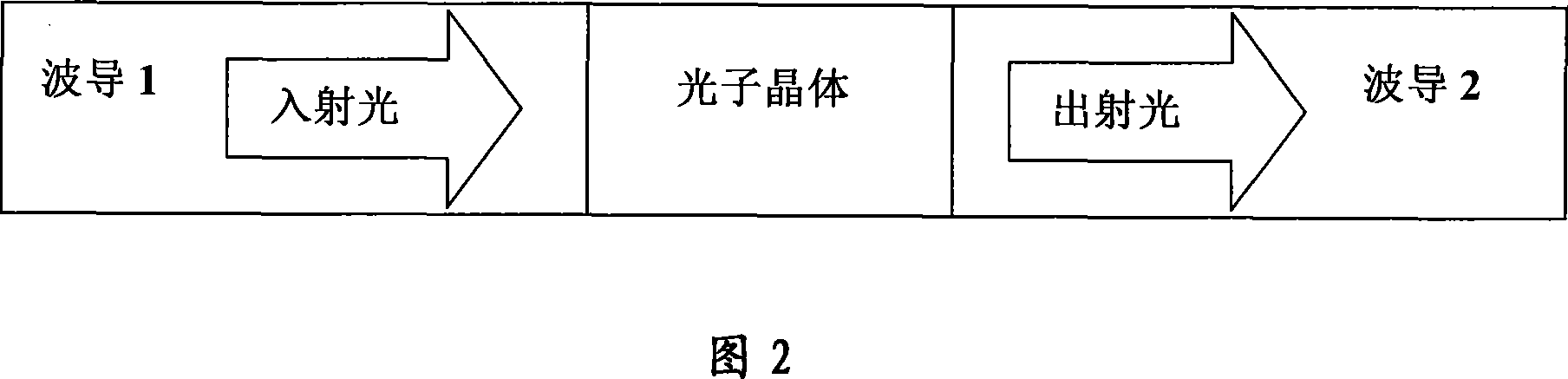
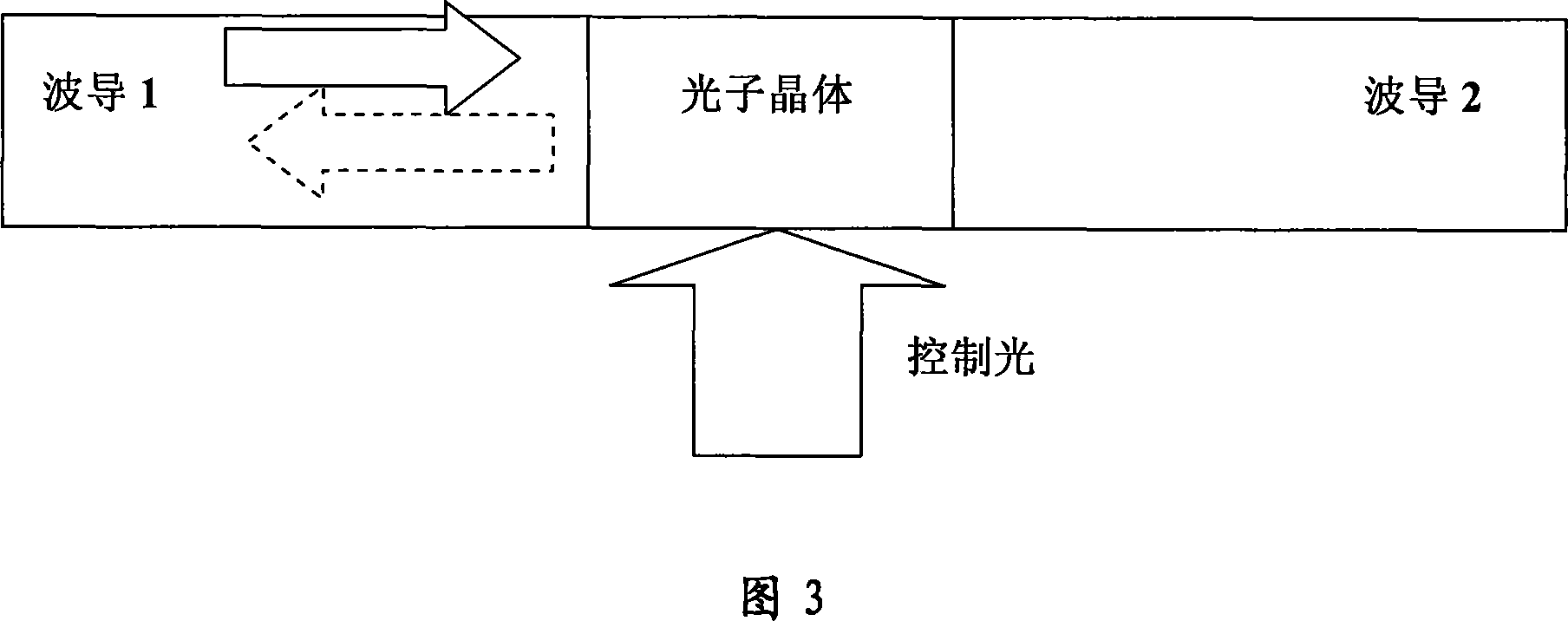
Image


Examples
Embodiment Construction
[0047] 1. Preparation of two-dimensional photonic crystals:
[0048] 1. Selection of laser dyes:
[0049] Laser dye of the present invention is divided into four classes according to chemical structure, (1) cyanine dye, its laser range is 540-1200nm; (2) coumarin dye, its laser range is 425-565nm; (3) oxazine class The dye has a laser range of 650-700nm; (4) the scintillation material is an aromatic compound containing oxazine, oxadiazole, and benzoxazole rings, and is a laser dye in the violet to ultraviolet region.
[0050] 2. Selection of organic conjugated polymers:
[0051] Organic conjugated polymers composed of chain molecules containing unsaturated covalent π bonds: such as polydiacetylene (PDA), polyacetylene (PA), polythiophene (PT), polystyrene (PS), etc.;
[0052] Organic conjugated polymers composed of unsaturated covalent π bonds and saturated covalent σ bonds alternately bonded to form large conjugated cyclic molecules: such as phthalocyanine, bufen, etc.;
...
PUM
| Property | Measurement | Unit |
|---|---|---|
| radius | aaaaa | aaaaa |
| thickness | aaaaa | aaaaa |
Abstract
Description
Claims
Application Information