Etching method of inclined through hole

A technology of hole wall and bottom surface, which is applied in the field of etching of inclined through holes to achieve the effect of easy metal filling

Pending Publication Date: 2021-07-20
BEIJING NAURA MICROELECTRONICS EQUIP CO LTD
View PDF0 Cites 0 Cited by
  • Summary
  • Abstract
  • Description
  • Claims
  • Application Information

AI Technical Summary

Problems solved by technology

[0003] The existing back through hole etching process generally directly adopts physical etching or chemical etching, and alternately performs physical etching and chemical etching, but this etching method will form a s

Method used


Image

  • Etching method of inclined through hole
  • Etching method of inclined through hole
  • Etching method of inclined through hole

Examples


Embodiment 1

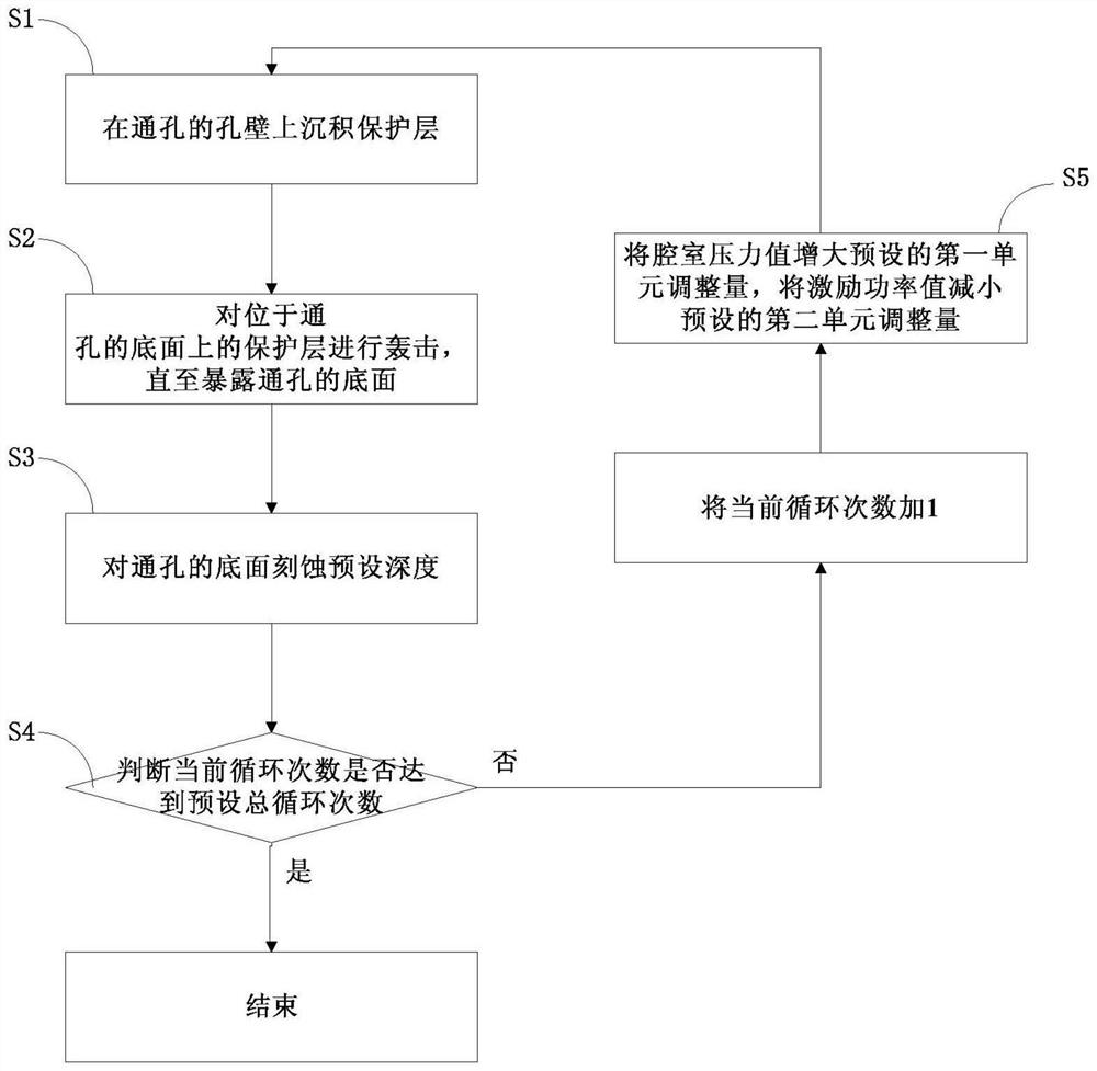
[0042] This embodiment provides an etching method for inclined through holes, which is used to etch through holes with inclined walls on a film layer made of a wide bandgap semiconductor material, the wide bandgap semiconductor material includes silicon carbide or nitrogen Gallium chloride, these two materials are representative of the third generation of semiconductor materials. However, this embodiment is not limited thereto, and the above etching method can also be used to etch holes on the surface of a film layer made of third-generation semiconductor materials such as zinc oxide or diamond.

[0043] The above-mentioned wide-bandgap semiconductor materials generally have the characteristics of high hardness, high brittleness, and high melting point. This characteristic makes it difficult to process holes with inclined angles in the wide-bandgap semiconductor material film layer. The current etching method only A straight hole or a hole with a very small inclination angle o...

Embodiment 2

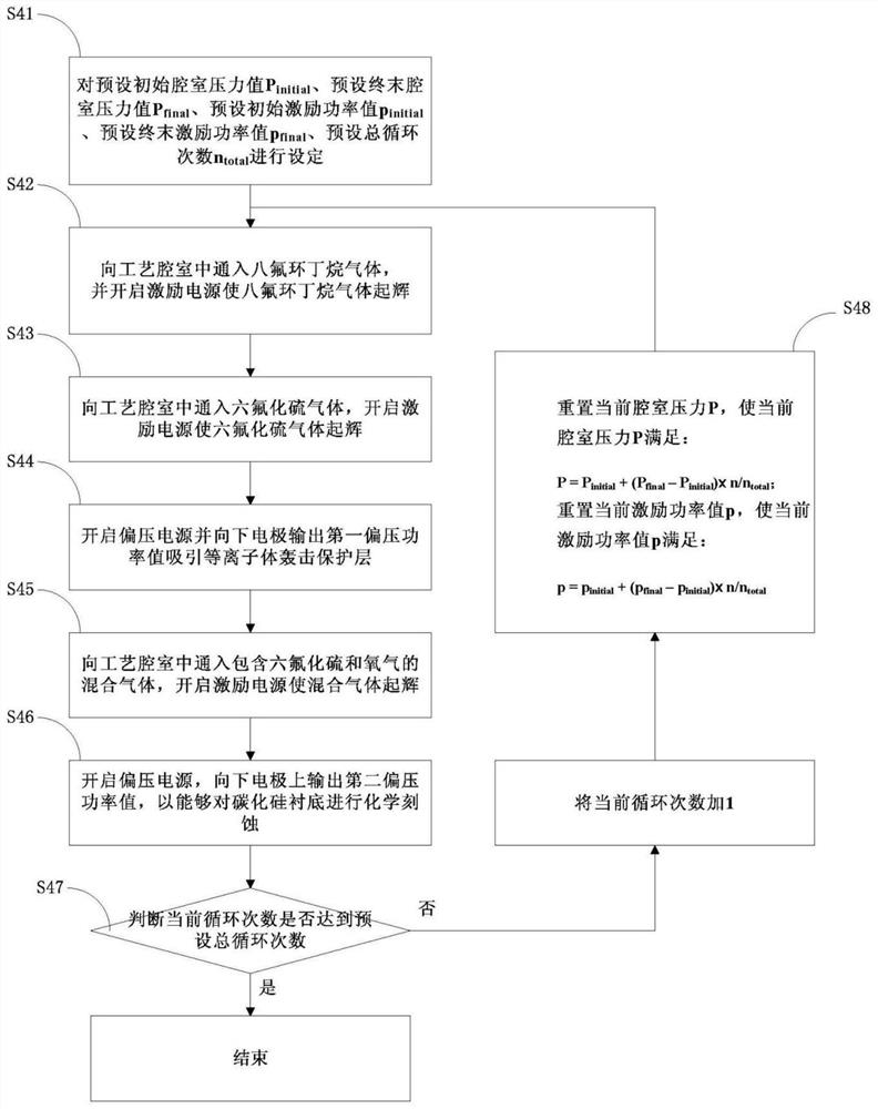
[0087] On the basis of Embodiment 1, this embodiment provides an etching method applied to an inclined through hole of a silicon carbide film layer, which specifically includes:

[0088] S41. For the preset initial chamber pressure value P initial , preset final chamber pressure value P final , preset initial excitation power value p initial , preset terminal excitation power value p final , preset total number of cycles n total make settings;

[0089] S42. Introduce octafluorocyclobutane gas into the process chamber, and turn on the excitation power to excite octafluorocyclobutane gas to form plasma. The plasma contains carbon ions and fluorine ions. Polymerization reaction can take place and generate fluorocarbon polymer, so that the fluorocarbon polymer is deposited on the surface of the film layer to form a protective layer;

[0090]Specifically, when performing the above step S42, the octafluorocyclobutane gas is simultaneously fed into the central air inlet and the ...

Embodiment 3

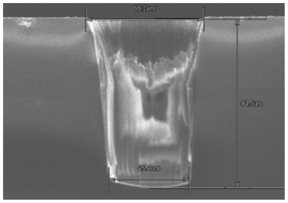
[0112] On the basis of Embodiment 1, this embodiment provides a method for etching through holes applied to gallium nitride film layers, such as Figure 4 As shown, it specifically includes:

[0113] S51. For the preset initial chamber pressure value P initial , preset final chamber pressure value P final , preset initial excitation power value p initial , preset terminal excitation power value p final , preset total number of cycles n total make settings;

[0114] S52. Introduce boron trichloride gas into the process chamber, turn on the excitation power to excite boron trichloride gas to form plasma, the plasma contains boron ions and chloride ions, wherein boron ions are catalyzed by high temperature and high pressure It will have a replacement reaction with the gallium nitride film layer, and generate a dense gallium boride compound on the gallium nitride film layer, so that the gallium boride compound can be deposited on the surface of the film layer to form a protec...


PUM


Abstract

The invention provides a method for etching an inclined through hole, which is used for etching a through hole with an inclined hole wall on a film layer made of a wide bandgap semiconductor material, and comprises the following steps: S1, depositing a protective layer on the hole wall of the through hole; S2, etching the protection layer on the bottom surface of the through hole until the bottom surface of the through hole is exposed; S3, etching the bottom surface of the through hole by a preset depth; S4, judging whether the current cycle index reaches a preset total cycle index or not, if not, adding 1 to the current cycle index, and performing the step S5; if yes, ending the process; and S5, increasing the pressure value of the cavity by a preset first unit adjustment amount, reducing the excitation power value by a preset second unit adjustment amount, and returning to the step S1. According to the etching method provided by the invention, the through hole with the hole wall with the specified inclination angle can be formed in the wide bandgap semiconductor material, so that a metal layer can be conveniently loaded in the through hole.

Description

technical field [0001] The invention relates to the field of semiconductor manufacturing, in particular to an etching method for inclined through holes. Background technique [0002] At present, the third-generation semiconductor materials are widely used in the field of semiconductor manufacturing because of their advantages such as large band gap, high breakdown electric field strength, and high saturation electron drift velocity. However, due to the poor thermal conductivity of some third-generation semiconductor materials (such as gallium nitride materials), when using third-generation semiconductor materials with poor thermal conductivity to make transistors, it is necessary to set back through holes on the film layer of the transistor. To assist heat dissipation, wherein, the back through hole is a surface hole opened on the surface of the film layer and communicated with the source and drain. The back via hole is usually filled with a metal layer, which can be used a...

Claims


Application Information

Patent Timeline
IPC IPC(8): H01L21/3065H01L21/308H01L21/04H01L21/48H01L21/768H01L23/367H01L23/46H01L21/67
CPCH01L21/0475H01L21/3065H01L21/30655H01L21/308H01L21/486H01L21/67276H01L21/76898H01L23/367H01L23/46
Inventor 林源为贺云瑞
Owner BEIJING NAURA MICROELECTRONICS EQUIP CO LTD
Why Eureka
Try Eureka