

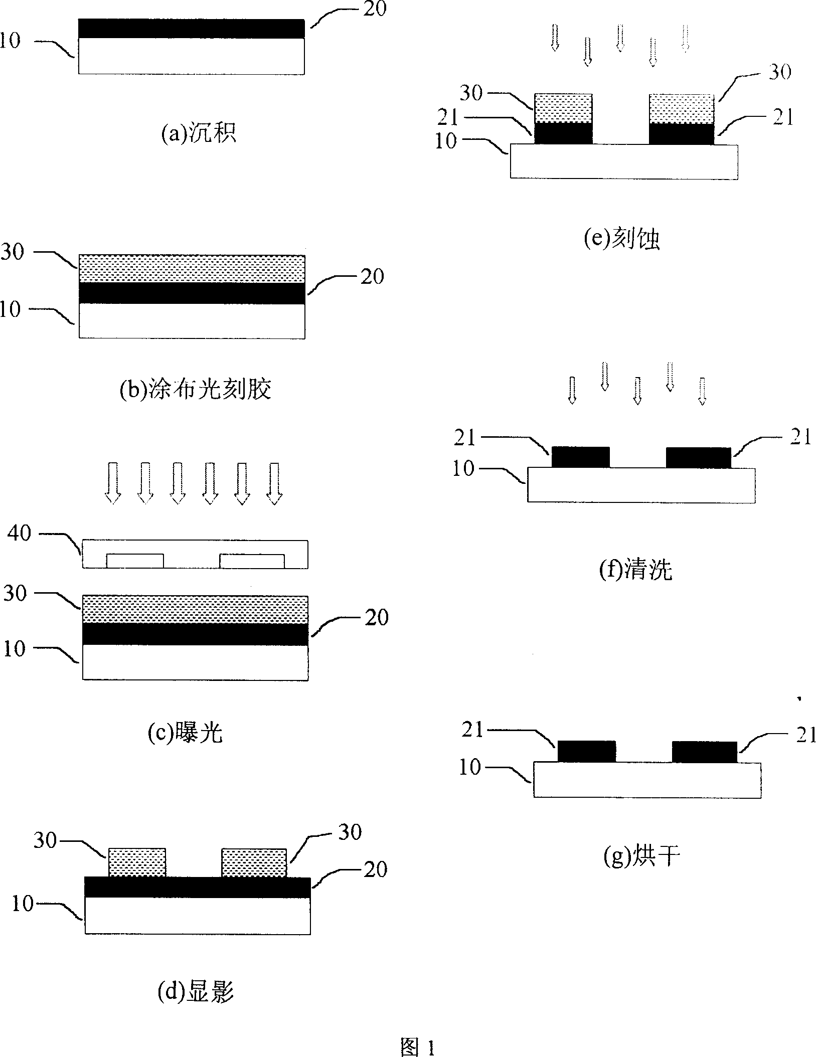
Making method of self-limited boundary film graphics
A technology of thin film graphics and boundaries, which is applied in the direction of conductive pattern formation, printed circuit manufacturing, semiconductor/solid-state device manufacturing, etc., can solve problems affecting the uniformity and flatness of thin film, performance degradation of thin film devices, and uneven film thickness, etc., to achieve Good smoothness and uniformity
- Summary
- Abstract
- Description
- Claims
- Application Information
AI Technical Summary
Problems solved by technology
Method used
Image

Examples
Embodiment 1
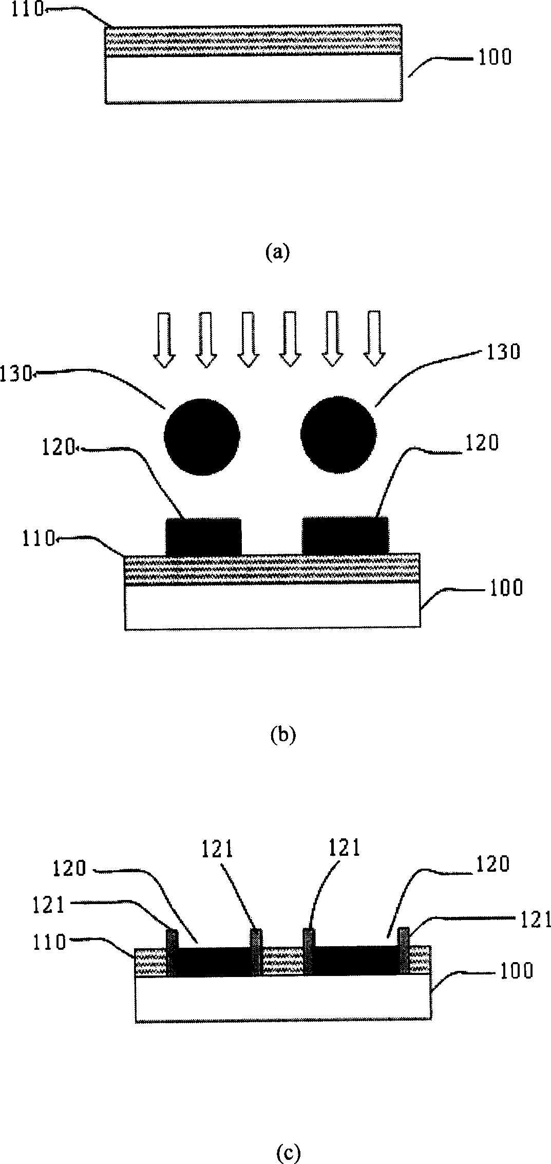
[0029] Embodiment 1: Please refer to the flow charts in Fig. 2(a) to Fig. 2(e).
[0030] First, as shown in FIG. 2( a ), a glass substrate 100 is provided and cleaned with deionized water, and a polymethyl methacrylate (PMMA) barrier layer 110 is preferably formed on the glass substrate 100 . The method for forming the PMMA barrier layer 110 may be spin coating or spinless coating. The silver nanoparticles are then dispersed in an acetone solvent to form a suspension 130 .
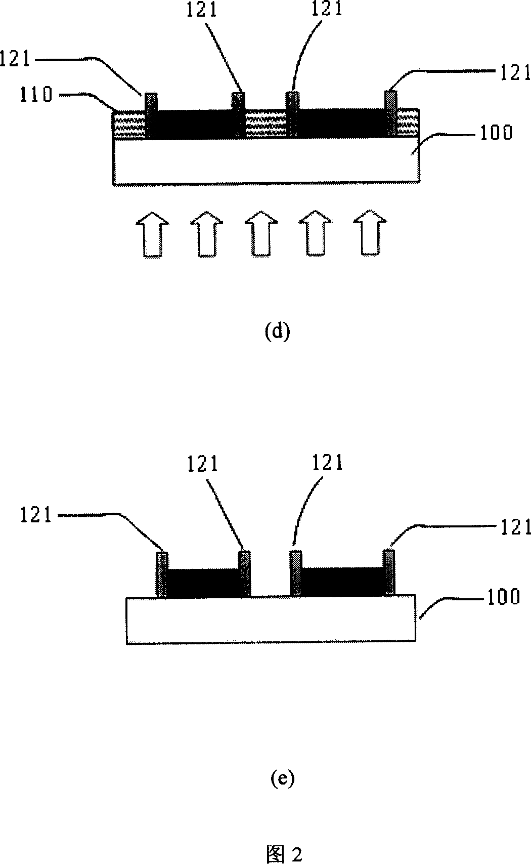
[0031] Then, please refer to shown in Figure 2 (b), the suspension 130 of silver nanoparticles is deposited on the top of the PMMA barrier layer 110, and patterning is carried out according to the prior design when depositing, here is a circular conductive pattern film 120 . The method of forming the conductive thin film layer 120 may be inkjet printing, or other wet film forming methods. Next, please refer to shown in Figure 2 (c), when the silver nano-suspension 130 is deposited on the top of the PMMA...
Embodiment 2
[0032] Embodiment 2, please also refer to the flowcharts of FIG. 2(a) to FIG. 2(e).
[0033] First, please refer to FIG. 2( a ), a glass substrate 100 is provided and cleaned with deionized water. A polyimide (PI) barrier layer 110 is formed on the glass substrate 100 , and the method for forming the barrier layer 110 may be spin coating (Spin Coating) or non-spin coating (Spinless Coating). The silver nanoparticles are then dispersed in a chloroform solvent to form a suspension 130 . Then, as shown in FIG. 2( b ), the suspension 130 of silver nanoparticles is deposited on the polyimide barrier layer 110 , and is patterned according to the prior design during deposition, which is a rectangle here. The method of forming the rectangular conductive thin film layer 120 may be inkjet printing, or other wet film forming methods.
[0034] Then please refer to Fig. 2 (c), when the silver nano-suspension 130 is deposited on the top of the polyimide barrier layer of the glass substrat...
PUM
| Property | Measurement | Unit |
|---|---|---|
| thickness | aaaaa | aaaaa |
| thickness | aaaaa | aaaaa |
Abstract
Description
Claims
Application Information