


Quick Research
Generate reliable direction feasibility study reports for your R&D in just a few steps.

Technical Q&A
Discover and master advanced knowledge NOW. Basics, ideas, possibilities, all at once.

Find Solutions
As an expert in R&D theories, this can generate solutions to your technical problems instantly.

Evaluate Feasibility
Analyze your overall solution with one click, know your potential R&D risks in advance.

Monitor Landscape
Get weekly tech updates, stay abreast of the latest tech innovations and key insights.
Light beam conversion shaping device for high power semiconductor laser array
A technology of beam shaping and beam conversion, which is applied in the direction of semiconductor laser devices, semiconductor lasers, laser devices, etc., can solve problems such as high cost, difficulty in design and production, and complex structure of micro-optical components, so as to achieve simple production and easy processing , low cost effect
- Summary
- Abstract
- Description
- Claims
- Application Information
AI Technical Summary
Problems solved by technology
Method used
Image


Examples
Embodiment 1
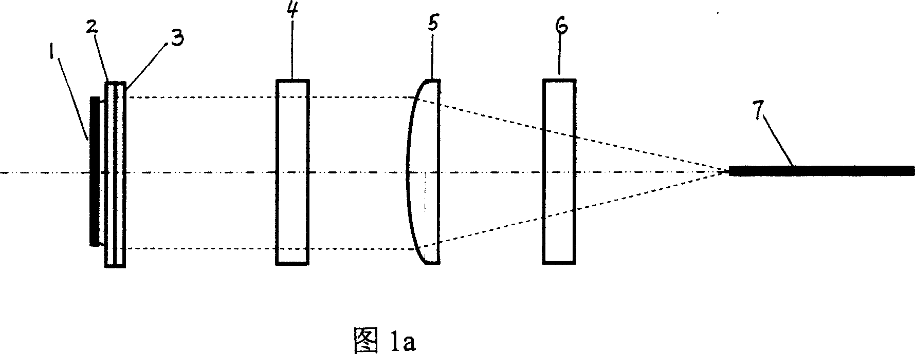
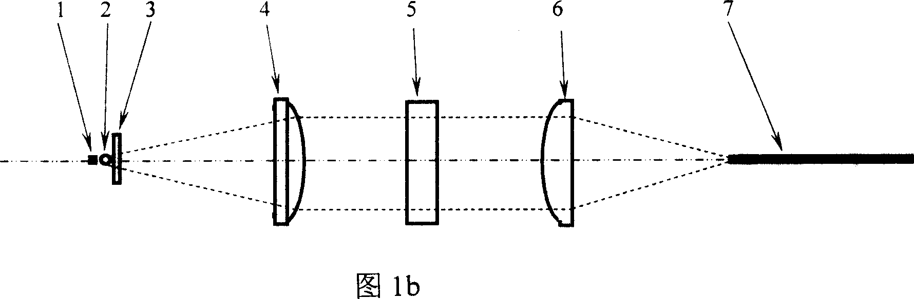
[0024] Referring to Fig. 1a and Fig. 1b, in the beam propagation direction of semiconductor semiconductor laser array 1, cylindrical lens 2 is placed in sequence, the input surface of cylindrical lens 2 is close to the output end of semiconductor laser array 1, and the output surface of cylindrical lens 2 is close to optical fiber array The input surface of the row 3, the output surface of the fiber array row 3 is close to the plane of the first cylindrical mirror 4, the cylindrical surface of the first cylindrical mirror 4 is close to the cylindrical surface of the second cylindrical mirror 5, and the second cylindrical mirror 5 The plane of the third cylindrical mirror 6 is close to the cylindrical surface of the third cylindrical mirror 6, and the plane of the third cylindrical mirror 6 is close to the input surface of the optical fiber 7.
[0025] The optical fiber array row 3 of this embodiment is made up of several silica optical fibers of the same diameter. In this embod...
Embodiment 2
[0028] The structure of the device made in this embodiment is the same as that of Example 1, wherein the optical fiber array row 3 is composed of several silica optical fibers with the same diameter, and 24 or 40 220 μm or 250 μm or 355 μm optical fibers can be used. The optical fiber array row 3 With respect to the cylindrical lens 2, the arrangement period is 500 μm at an angle of 45 degrees. Other parameters are the same as in Example 1.
Embodiment 3
[0030]The structure of the device produced in this embodiment is the same as that of Embodiment 1, wherein the optical fiber array row 3 can be composed of several glass filaments of the same diameter, and each glass filament in the optical fiber array row 3 is arranged at an angle of 45 degrees relative to the cylindrical lens 2. Other parameters are the same as in Example 1.
PUM
 Abstract
Description
Claims
Application Information
 - R&D Engineer
- R&D Manager
- IP Professional
- Industry Leading Data Capabilities
- Powerful AI technology
- Patent DNA Extraction
Browse by: Latest US Patents, China's latest patents, Technical Efficacy Thesaurus, Application Domain, Technology Topic, Popular Technical Reports.
© 2024 PatSnap. All rights reserved.Legal|Privacy policy|Modern Slavery Act Transparency Statement|Sitemap|About US| Contact US: help@patsnap.com