Check patentability & draft patents in minutes with Patsnap Eureka AI!

Semiconductor device and its making method

A manufacturing method and semiconductor technology, which can be used in the manufacture of semiconductor/solid-state devices, semiconductor devices, semiconductor/solid-state device components, etc., can solve problems such as poor adhesion and peeling, and achieve the effect of reducing corrosion and damage and increasing adhesion.

Active Publication Date: 2007-10-31
SEMICON MFG INT (SHANGHAI) CORP +1
View PDF1 Cites 23 Cited by
  • Summary
  • Abstract
  • Description
  • Claims
  • Application Information

AI Technical Summary

Problems solved by technology

[0006] Therefore, the object of the present invention is to provide a semiconductor device and its manufacturing method, to solve the problem of poor adhesion between the top metal interlayer and its lower etch stop layer and peeling off

Method used


Image

  • Semiconductor device and its making method
  • Semiconductor device and its making method
  • Semiconductor device and its making method

Examples


Embodiment Construction

[0043] In order to make the above objects, features and advantages of the present invention more comprehensible, specific implementations of the present invention will be described in detail below in conjunction with the accompanying drawings.

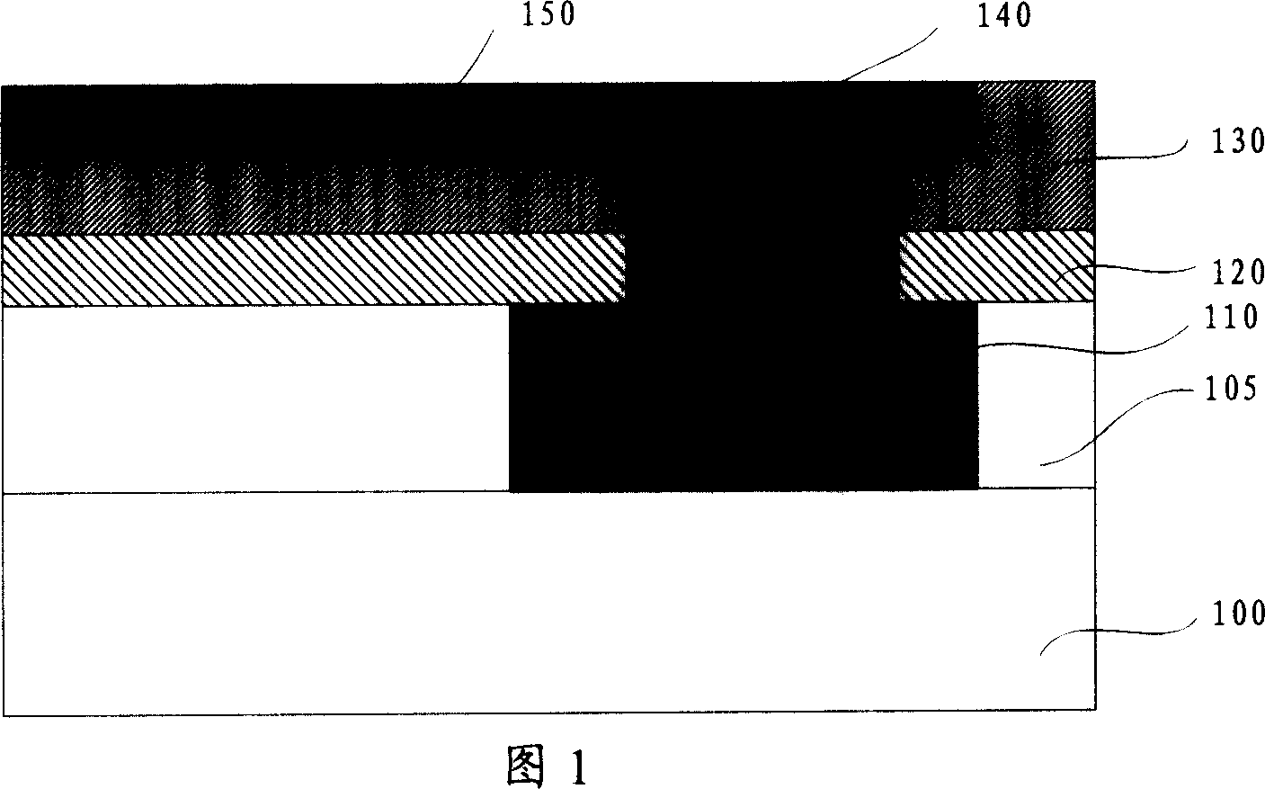
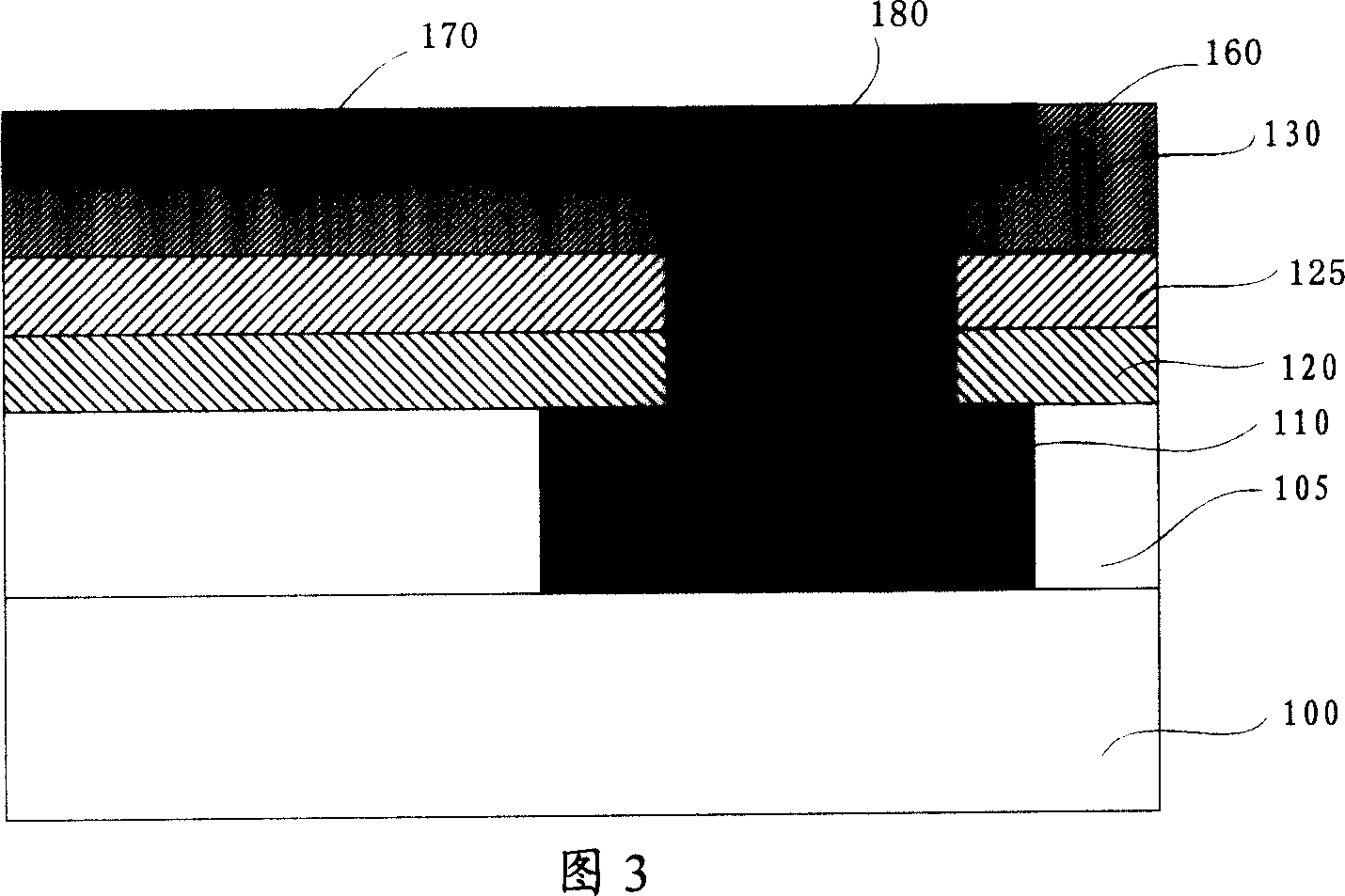
[0044] Fig. 3 is a cross-sectional view of the structure of the semiconductor device of the present invention. As shown in Figure 3, the semiconductor device of the present invention includes a substrate 100 and a metal pattern layer 110 formed in a dielectric layer 105 on the substrate 100, and the metal pattern layer 110 is formed by spin-coating a photoresist on the dielectric layer 105. It is formed by exposure, development and etching of photoresist. An etch stop layer 120 is formed on the dielectric layer 105 and the metal pattern layer 110 with a thickness of 100 angstroms to 300 angstroms, and its material can be silicon oxide, silicon carbide (SiC), silicon nitride (SiN), carbon nitride Oxygen compound (SiOC), one or a combin...


PUM

PropertyMeasurementUnit
Thicknessaaaaaaaaaa
Thicknessaaaaaaaaaa

Abstract

The invention provides semiconductor component and preparing method. The semiconductor component possesses a top metal layer and a lower metal layer which is electric connected with the top metal layer via the middle medium layer. The method firstly covers etch stopping layer on the underlay which possesses metal pattern, its thickness is 100-300 angstrom, covering the blocking layer whose thickness is two times of etch stopping layer on the etch stopping layer, covering middle medium layer on the blocking layer and etching the groove and through hole which are needed by depositing top metal, thereinto existence of the blocking layer avoids peeling off of the etch stopping layer and the middle medium layer.

Description

technical field [0001] The invention relates to the technical field of semiconductor manufacturing, in particular to a semiconductor device and a manufacturing method thereof. Background technique [0002] While the development of semiconductor technology requires higher and higher integration, the requirements for line width and process are also becoming more and more stringent. While moving towards small line width technology nodes, the IC industry chooses copper and low-K materials as the key solution to reduce the interconnect resistance capacitance (RC) delay of 0.13um and below technology nodes. In the process of removing aluminum, copper has the characteristics of easy diffusion and difficult etching. The industry has introduced the dual damascene process (Dual Damascene), which is characterized by first forming an intermediate dielectric layer on the substrate with devices and etching trenches and vias, then deposit copper into the etched pattern, and apply a planar...

Claims


Application Information

Patent Timeline
IPC IPC(8): H01L23/522H01L21/768
Inventor 张弓陈玉文卑多慧孙智江
Owner SEMICON MFG INT (SHANGHAI) CORP
Features
  • R&D
  • Intellectual Property
  • Life Sciences
  • Materials
  • Tech Scout
  • Unparalleled Data Quality
  • Higher Quality Content
  • 60% Fewer Hallucinations
Learn More