

P+PIN silicon photoelectric probe
A detector, silicon photoelectric technology, applied in circuits, electrical components, semiconductor devices, etc., can solve the problems of low response to short-wave light and small photogenerated current of PIN photodetectors
- Summary
- Abstract
- Description
- Claims
- Application Information
AI Technical Summary
Problems solved by technology
Method used
Image

Examples
Embodiment Construction
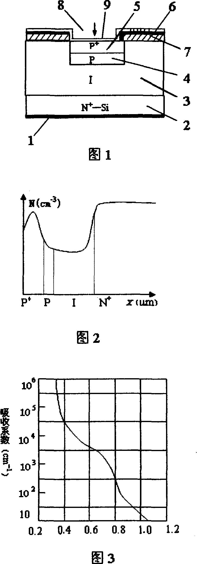
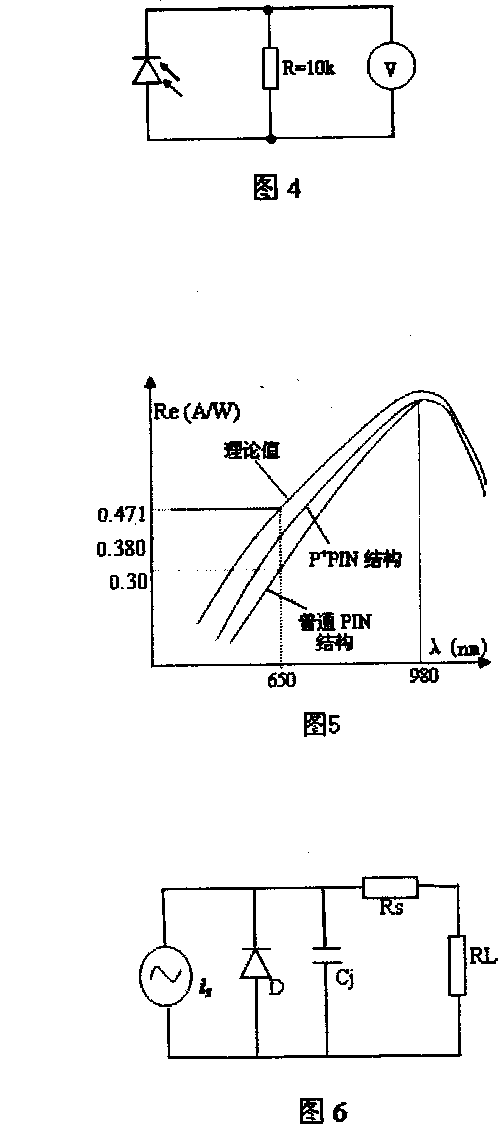
[0015] Referring to Fig. 1, P of the present invention + PIN silicon photodetectors consist of lower N + Layer 2, non-doped intrinsic layer 3 in the middle, containing P in the upper part + The boron diffusion region of the type concentrated boron diffusion layer 5 . Among them, N + The lower surface of the layer 2 is provided with an N-type ohmic contact layer 1 for connecting the positive electrode of an external power supply, and the N-type ohmic contact layer 1 is formed by sputtering aluminum (Al). The upper end of the non-doped intrinsic layer 3 is provided with an insulating layer 7, and the insulating layer is provided with a + The P-type ohmic contact layer 6 in contact with the P-type concentrated boron diffusion layer 5 is used to connect the negative electrode of the external power supply, and the P-type ohmic contact layer is also formed by sputtering aluminum (Al). There is an incident light window 8 formed by photolithography on the insulating layer, so that...
PUM
 Abstract
Description
Claims
Application Information