Novel packaging system and method for organic electroluminescence device

An electroluminescent device and packaging system technology, which is applied in the direction of electro-solid devices, electrical components, semiconductor devices, etc., can solve problems such as inability to meet or be compatible with OLED devices, and achieve simple and reasonable structure, improved life, and reduced water vapor and oxygen penetration. rate effect

Inactive Publication Date: 2008-01-02
UNIV OF ELECTRONICS SCI & TECH OF CHINA
View PDF0 Cites 11 Cited by
  • Summary
  • Abstract
  • Description
  • Claims
  • Application Information

AI Technical Summary

Problems solved by technology

So far, there are certain problems in the packaging methods of OLED devices. The existing methods o

Method used


Image

  • Novel packaging system and method for organic electroluminescence device
  • Novel packaging system and method for organic electroluminescence device

Examples


Embodiment approach 1-7

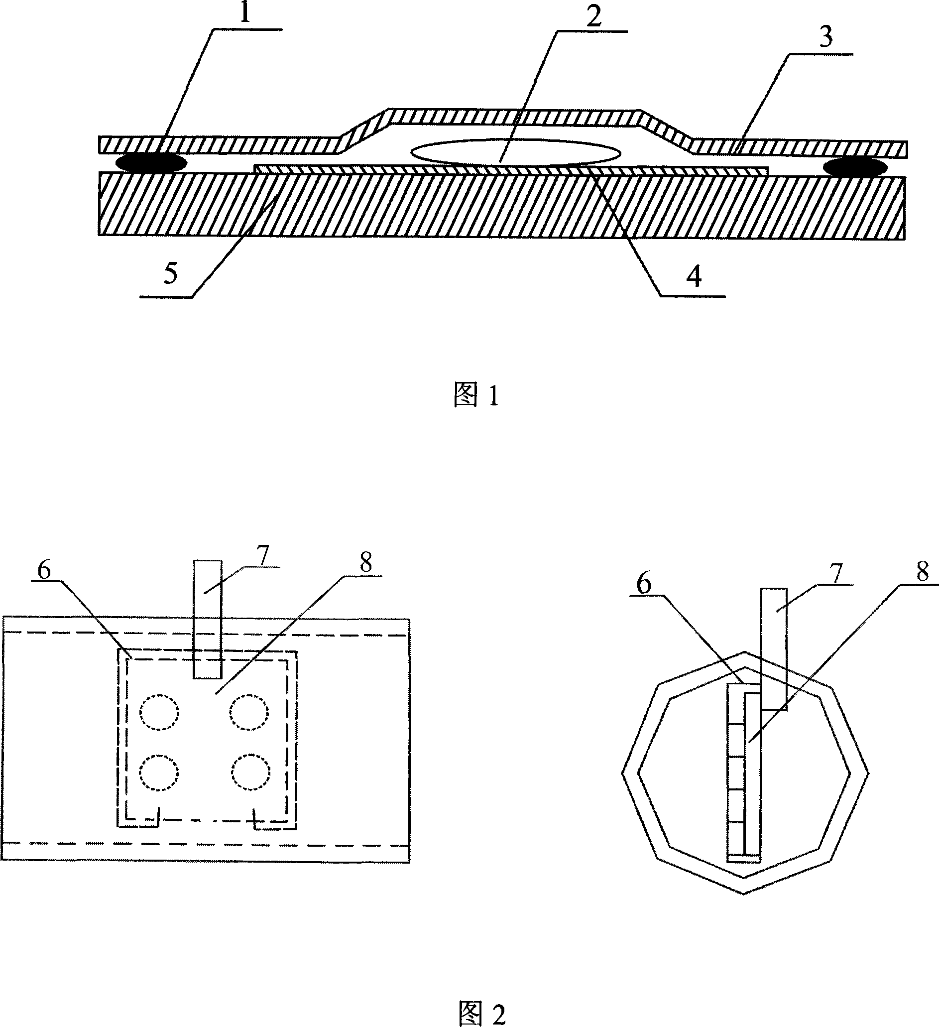
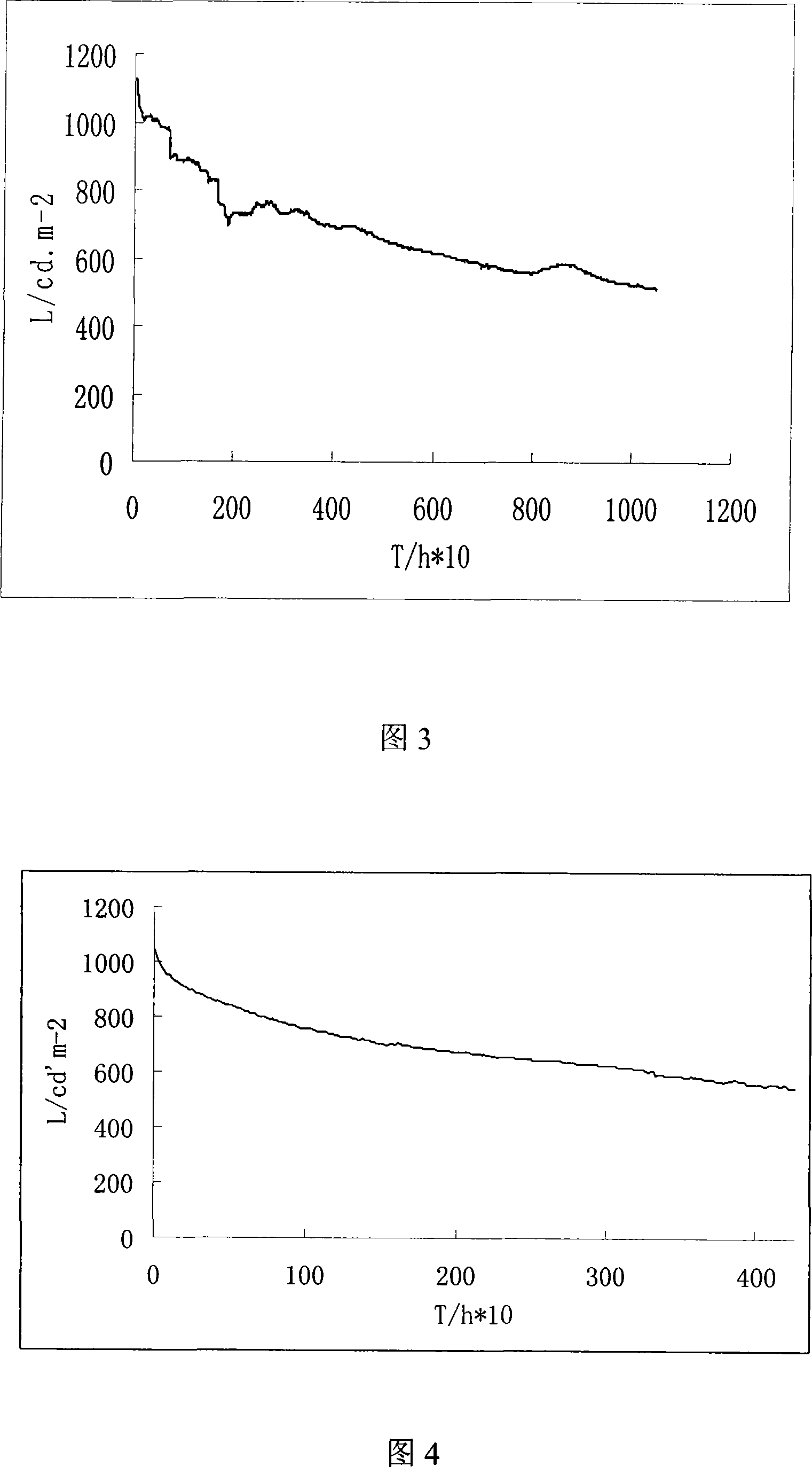
[0032] The basic structure of the organic electroluminescent device (OLED) packaging system is shown in Figure 1. The device substrate is a 200mm×200mm glass substrate, the packaging cover is etched with soda-lime glass, and the sealant is UV-curable. The entire device structure is described as: glass substrate / ITO / CuPc (200 Ȧ) / α-NPD (600 Ȧ) / Alq 3 (400 Ȧ): C545T (2%) / Alq3 (200A) / LiF(10A) / Al(1000A). The preparation method is as follows:

[0033] ①Use detergent, ethanol solution and deionized water to ultrasonically clean the transparent conductive substrate ITO glass, and dry it with dry nitrogen after cleaning. Wherein the ITO film on the glass substrate is used as the anode layer of the device, the square resistance of the ITO film is 10-15Ω / □, and the film thickness is 1500 Ȧ;

[0034] ② Move the dried substrate into a high-vacuum chamber, and pretreat the ITO glass with low-energy oxygen plasma for 10 minutes in an oxygen and argon atmosphere with a pressure of 20Pa, and ...

specific Embodiment approach 8-14

[0042] The basic structure of the organic electroluminescent device (OLED) packaging system is shown in Figure 1. The device substrate is a 200mm×200mm glass substrate, the packaging cover is etched with soda-lime glass, and the sealant is UV-curable. The entire device structure is described as: glass substrate / ITO / CuPc (200 Ȧ) / α-NPD (600 Ȧ) / Alq 3 (400 Ȧ): C545T (2%) / Alq 3 (200A) / LiF(10A) / Al(1000A).

[0043] The preparation method is as follows:

[0044] ①Use detergent, ethanol solution and deionized water to ultrasonically clean the transparent conductive substrate ITO glass, and dry it with dry nitrogen after cleaning. Wherein the ITO film on the glass substrate is used as the anode layer of the device, the square resistance of the ITO film is 10-15Ω / □, and the film thickness is 1500 Ȧ.

[0045] ② Move the dried substrate into a high-vacuum chamber, and pretreat the ITO glass with low-energy oxygen plasma for 10 minutes in an oxygen and argon atmosphere with a pressure of...

specific Embodiment approach 15-21

[0053] The basic structure of the organic electroluminescent device (OLED) packaging system is shown in Figure 1. The device substrate is a flexible substrate (such as PET, etc.), the packaging cover is etched with soda-lime glass, and the sealant is UV-curable. The entire device structure is described as: glass substrate / ITO / CuPc (200 Ȧ) / α-NPD (600 Ȧ) / Alq 3 (400 Ȧ): C545T (2%) / Alq 3 (200A) / LiF(10A) / Al(1000A).

[0054] The fabrication process of the device is similar to Embodiments 1-7.


PUM

PropertyMeasurementUnit
Sheet resistanceaaaaaaaaaa

Abstract

The invention discloses a novel package system of organic electroluminescent device, comprising a baseboard composed of a substrate and an organic electroluminescent working layer, wherein the organic electroluminescent working layer comprises an anode layer, a cavity transmission layer, an electron transmission layer, and a metal electrode. The invention is characterized in that the substrate is arranged with a cover board at the side plated with the organic electroluminescent working layer, the cover board and the substrate seal the organic electroluminescent working layer via ultrasonic exposure adhesive, wherein the gas pressure in the ultrasonic exposure adhesive sealed area is lower than external pressure, to tightly and uniformly combine the cover board and the baseboard. The invention can effectively reduce steam and oxygen penetration factor which can reach 10-6g/m2/day at 65Deg. C and 97% humidity, while the device service life is improved to 10 thousand hours from prior 3000-5000h, to meet practical application.

Description

technical field [0001] The invention relates to an organic electroluminescent device, in particular to a novel packaging system and packaging method of the organic electroluminescent device and related equipment. Background technique [0002] Organic Light-Emitting Diode (OLED) is a technology that can emit light by itself by applying a voltage. Because organic compounds can emit light by themselves, unlike liquid crystal displays, which must be transparent on the back to display, organic light-emitting displays do not need to be equipped with light-emitting diodes on the back, and can be made thinner and lighter. system on clothes. Organic light-emitting display also has the advantages of high brightness, wide viewing angle, low voltage drive, low power consumption, fast response speed, no afterimage, low production cost, simple manufacturing process, good resolution and high brightness, and is considered to be the next generation. The emerging application technology of f...

Claims


Application Information

Patent Timeline
IPC IPC(8): H01L51/50H01L51/56H01L23/10H01L23/28H01L21/50H01L21/52H01L21/56
Inventor 钟建于军胜蒋亚东
Owner UNIV OF ELECTRONICS SCI & TECH OF CHINA
Why Eureka
Try Eureka