
Semiconductor device and method of manufacturing the same

A semiconductor and crystal technology, which is applied in the field of field effect transistor semiconductor devices, can solve the problems of performance degradation, component performance fluctuations, and the crystallinity of the TFT channel formation region cannot be strictly controlled, so as to achieve the effect of reducing fluctuations and eliminating the causes of fluctuations

Inactive Publication Date: 2008-01-23
SEMICON ENERGY LAB CO LTD
View PDF5 Cites 0 Cited by
  • Summary
  • Abstract
  • Description
  • Claims
  • Application Information

AI Technical Summary

Problems solved by technology

[0010] For example, when a semiconductor film is formed on a glass substrate to construct a TFT, the TFT is arranged regardless of arbitrarily formed grain boundaries, and thus the crystallinity of the TFT channel formation region cannot be strictly controlled
Randomly formed crystal defects at grain boundaries degrade performance and cause fluctuations in performance between components

Method used


Image

  • Semiconductor device and method of manufacturing the same
  • Semiconductor device and method of manufacturing the same
  • Semiconductor device and method of manufacturing the same

Examples


Embodiment approach 1

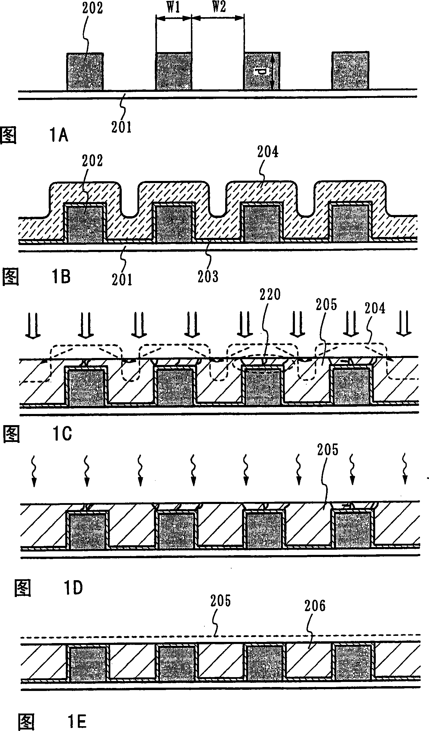
[0097] Referring to Figs. 1A-1E, description will be given in accordance with the above-described mode of the present invention. 1A-1E are vertical sectional views illustrating the process of forming the crystalline semiconductor film of the present invention.

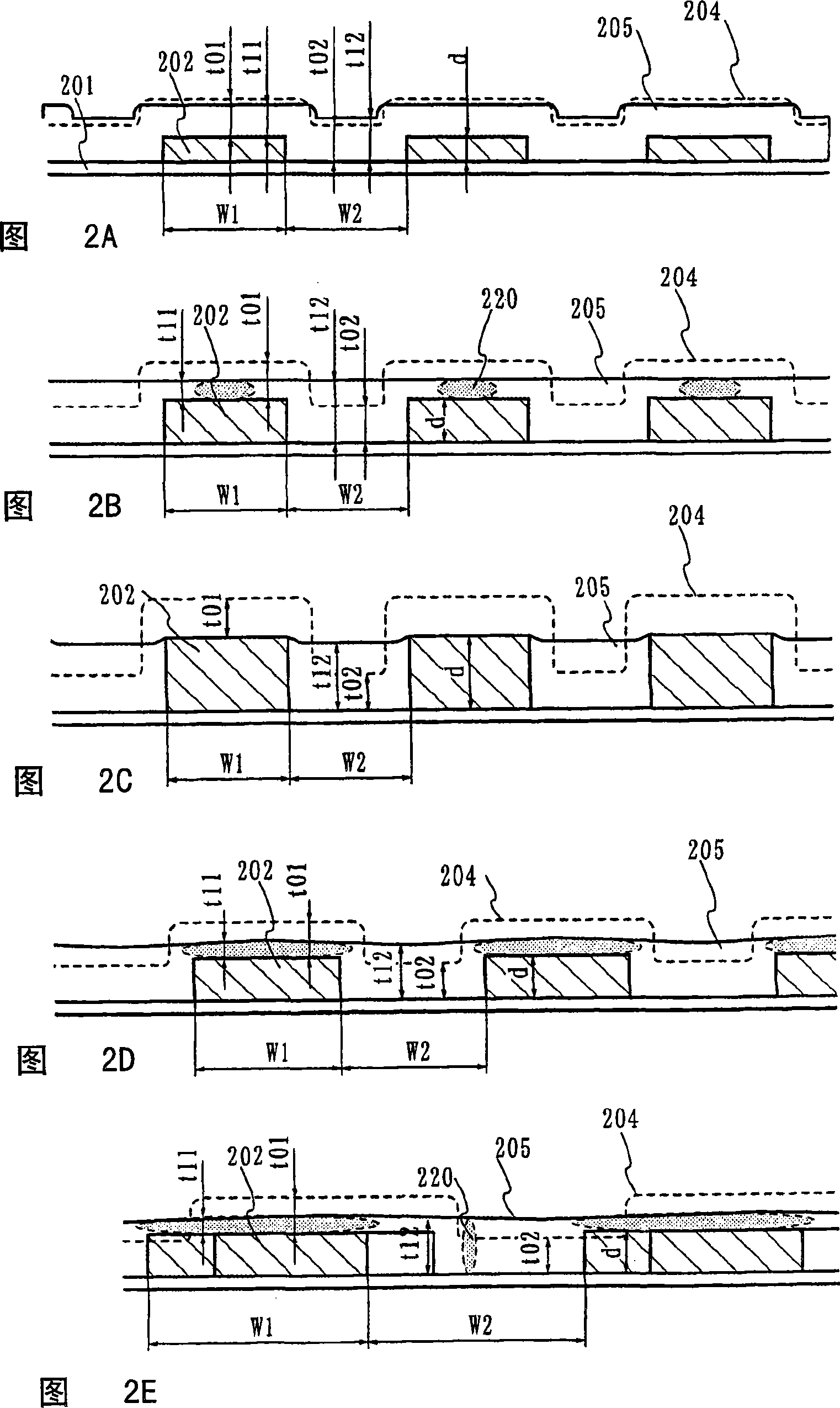
[0098] In FIG. 1A, the first insulating film 201 is formed to 30-300 nm using silicon nitride, silicon oxynitride having a nitrogen content higher than that of oxygen, aluminum nitride, or aluminum oxynitride. On the first insulating film 201, a second insulating film 202 is formed using silicon oxide or silicon oxynitride to a thickness of 10-1000 nm, preferably 50-200 nm. The second insulating film 202 has an opening of a desired shape. The desired shape may be a rectangle, a circle, a polygon, a strip, or a shape matching the shape of the TFT island-like semiconductor film (active layer) to be manufactured. Silicon oxide films can be prepared by plasma CVD with tetraethylorthosilicate (TEOS) and O 2 mixture forme...

Embodiment approach 2

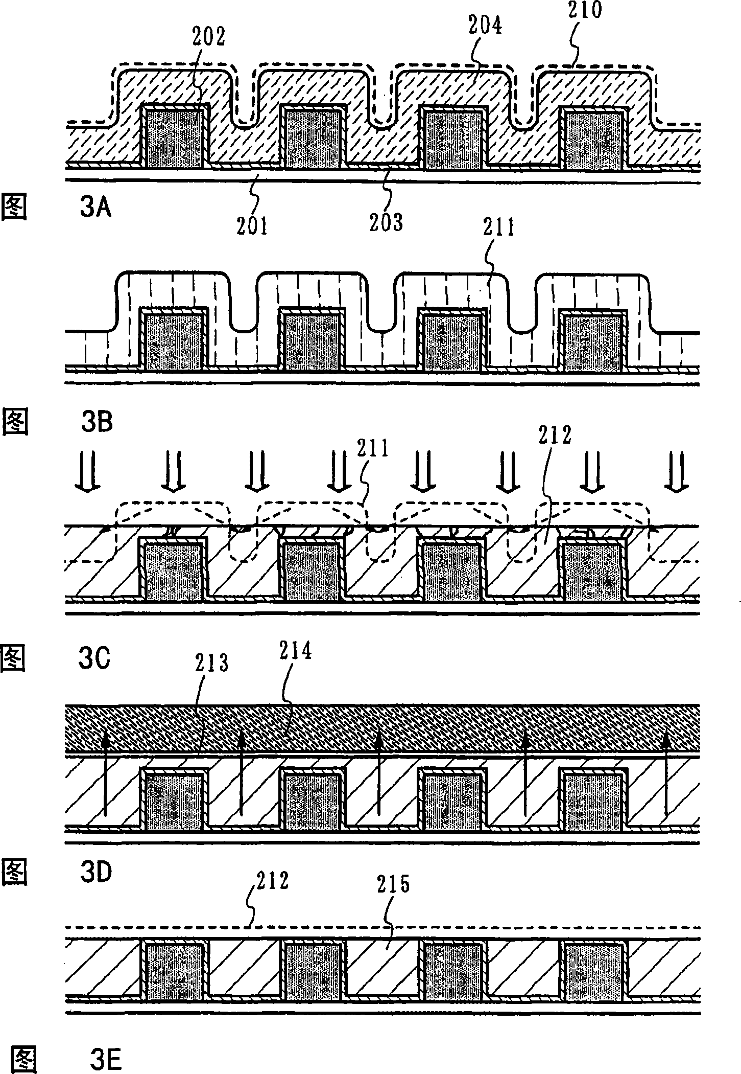
[0117] When forming the crystalline semiconductor film of the present invention, the amorphous semiconductor film crystallized by laser irradiation as shown in Embodiment 1 may be further irradiated with laser light to melt the film again for recrystallization.

[0118] 3A-3E show examples thereof. First, the first insulating film 201, the second insulating film 202, the silicon oxynitride film 203, and the amorphous semiconductor film 204 are formed in the manner described in Embodiment 1. The amorphous semiconductor film 204 is doped with Ni as a metal element having a catalytic effect to accelerate crystallization, such as lowering the crystallization temperature of silicon and improving orientation. How to dope with Ni is not limited, and spin coating, evaporation, sputtering, or other methods may be used. When spin coating is used, an aqueous solution containing 5-10 ppm nickel acetate is applied to form the layer 210 containing the metal element. The catalytic element ...

Embodiment approach 3

[0124]This embodiment gives a description of manufacturing a TFT pattern in which a channel formation region is placed in a filling region with reference to FIGS. 4A to 10F. The filling region is a region of the crystalline silicon film that fills an opening of the base insulating film formed under the crystalline silicon film. FIG. 4A is a plan view, and FIG. 4B and subsequent figures are vertical cross-sectional views of various parts of FIG. 4A. Similarly, Figures 5A, 6A, 7A, 8A, 9A and 10A are top views and the rest are vertical cross-sectional views.

[0125] In FIGS. 4A-4E , an aluminum oxynitride film or a silicon nitride film with a thickness of 30-300 nm is formed on a glass substrate 301 as a first insulating film 302 . On the first insulating film 302, a silicon oxide film or a silicon oxynitride film is formed and subjected to photolithography to form a second insulating film 303 having a rectangular pattern. The 1000 nm-thick silicon oxide film is coated with TEO...


PUM


Abstract

An objective is to provide a method of manufacturing a semiconductor device, and a semiconductor device manufactured by using the manufacturing method, in which a laser crystallization method is used that is capable of preventing the formation of grain boundaries in TFT channel formation regions, and is capable of preventing conspicuous drops in TFT mobility, reduction in the ON current, and increases in the OFF current, all due to grain boundaries. Depressions and projections with stripe shape or rectangular shape are formed. Continuous wave laser light is then irradiated to a semiconductor film formed on an insulating film along the depressions and projections with stripe shape of the insulating film, or along a longitudinal axis direction or a transverse axis direction of the rectangular shape. Note that although it is most preferable to use continuous wave laser light at this point, pulse wave laser light may also be used.

Description

field of invention [0001] The present invention relates to a semiconductor device formed of a semiconductor film having a crystalline structure and a method of manufacturing the semiconductor device, and more particularly, to a semiconductor device including a field effect transistor whose channel formation region is formed of a crystalline semiconductor film on an insulating surface and to manufacturing The semiconductor device method. Background of the invention [0002] There is known a technique of forming an amorphous semiconductor film on a glass or other insulating film substrate and crystallizing the film by irradiating laser light. A thin film transistor (hereinafter referred to as TFT) manufactured from a semiconductor film having a crystalline structure (crystalline semiconductor film) is applied to a flat display device (flat panel display), typically a liquid crystal display device. [0003] Laser light is used in semiconductor manufacturing processes in the fo...

Claims


Application Information

Patent Timeline
Patent Type & Authority Applications(China)
IPC IPC(8): H01L27/12H01L29/786
Inventor 矶部敦生山崎舜平小久保千穗田中幸一郎下村明久荒尾达也宫入秀和
Owner SEMICON ENERGY LAB CO LTD
Learn More