Organic electroluminescent device capable of emitting white light and method for fabricating the same

An electroluminescence and white light technology, applied in the fields of electro-solid devices, semiconductor/solid-state device manufacturing, electrical components, etc., can solve the problems of difficult to repeat device performance, high manufacturing costs, affecting industrialization, etc. , the effect of fast response

Inactive Publication Date: 2008-01-30
UNIV OF ELECTRONICS SCI & TECH OF CHINA
View PDF0 Cites 10 Cited by
  • Summary
  • Abstract
  • Description
  • Claims
  • Application Information

AI Technical Summary

Problems solved by technology

At present, the complex device structure and manufacturing process have seriously affected its industrialization, and the high manufacturing cost and difficult-to-repeat device performance h...

Method used


Image

  • Organic electroluminescent device capable of emitting white light and method for fabricating the same
  • Organic electroluminescent device capable of emitting white light and method for fabricating the same

Examples


Embodiment 1

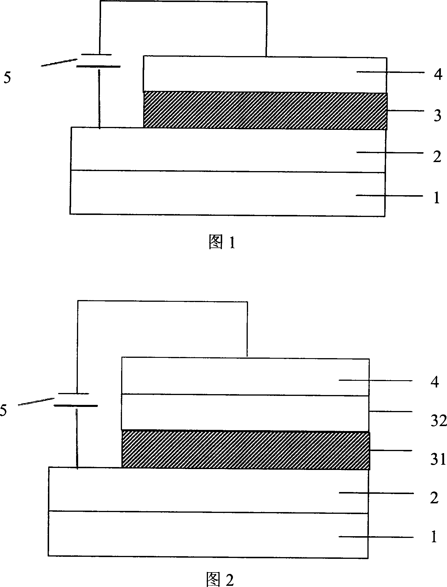
[0061] As shown in FIG. 1 , the hole transport layer in the structure of the device doubles as the white light emitting layer 3 .

[0062] The material of the hole transport layer of the device and also as the white light-emitting layer is PVK:NPB, and the cathode layer is made of Mg:Ag alloy. The entire device structure is described as:

[0063] Glass substrate / ITO / PVK:NPB(80nm) / Mg:Ag(200nm)

[0064] The preparation method is as follows:

[0065] ①Use detergent, ethanol solution, acetone solution and deionized water to ultrasonically clean the conductive substrate ITO glass, and dry it with dry nitrogen after cleaning. Wherein the ITO film on the glass substrate is used as the anode layer of the device, the square resistance of the ITO film is 10Ω / □, and the film thickness is 180nm.

[0066] ② Move the dried substrate into a vacuum chamber, and pretreat the ITO glass with low-energy oxygen plasma for 10 minutes under an oxygen pressure environment with an air pressure of 2...

Embodiment 2

[0073] As shown in FIG. 2 , the organic layer 3 in the structure of the device includes a hole transport layer also serving as a white light emitting layer 31 , and a hole blocking layer also serving as an electron transport layer 32 .

[0074] The hole transport layer of the device also serves as the white light-emitting layer material is PVK:NPB, the hole blocking layer also serves as the electron transport material BCP, and the cathode layer uses Mg:Ag alloy. The entire device structure is described as:

[0075] Glass substrate / ITO / PVK:NPB(80nm) / BCP(20nm) / Mg:Ag(100nm)

[0076] The fabrication process of the device is similar to that of Example 1.

Embodiment 3

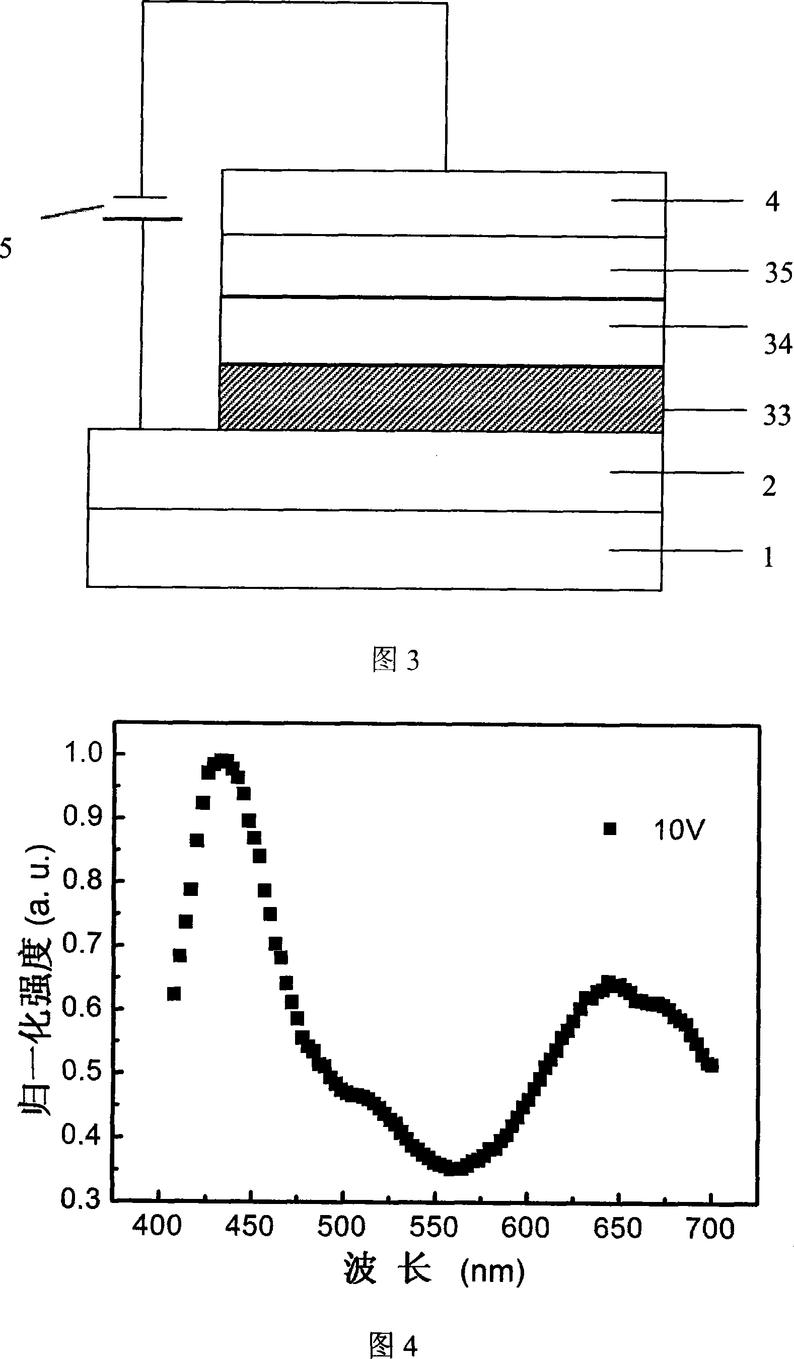
[0078] As shown in FIG. 3 , the organic layer 3 in the structure of the device includes a hole transport layer also serving as a white light emitting layer 33 , a hole blocking layer 34 and an electron transport layer 35 .

[0079] The material of the hole transport layer and the white light emitting layer of the device is PVK:NPB, the hole blocking material BCP, and the electron transport material Alq 3 , The cathode layer is made of Mg:Ag alloy. The entire device structure is described as:

[0080] Flexible substrate / ITO / PVK:NPB(80nm) / BCP(20nm) / Alq 3 (10nm) / Mg:Ag(100nm)

[0081] The fabrication process of the device is similar to that of Example 1.


PUM

PropertyMeasurementUnit
Sheet resistanceaaaaaaaaaa
Film thicknessaaaaaaaaaa

Abstract

The invention discloses an organic electroluminescent device which can give out light, comprising an organic electroluminescent device or a substrate, an anode layer and a cathode layer, and an electrode on the surface of the substrate, an organic functional layer between the anode layer and the cathode layer that comprises at least a luminescent layer which is an organic material layer giving out white light driven by an additional power, and is characterized in that the organic material layer giving out white light is made up by a plurality of blue organically functional materials with hole-transporting ability, the blue organically functional material can be one or more materials of aromatic diamines compounds, star-shaped triphenyl-amine compounds, carbazole polymer and metal complexes, DPVBi, BCzVB, Perylene and BczVBi.

Description

technical field [0001] The invention relates to the technical field of organic electroluminescence in electronic components, in particular to an organic electroluminescence device capable of emitting white light. Background technique [0002] The development of organic electroluminescent technology provides technical support and guarantee for micro-display or large-area information display, because organic electroluminescent displays have significant advantages: self-luminescence, low-voltage DC drive, high and low temperature resistance, full curing, wide viewing angle, Rich colors, no need for backlight, large viewing angle, low power, and a response speed up to 1000 times that of liquid crystal displays, but its manufacturing cost is much lower than that of liquid crystal displays with the same performance. Therefore, organic electroluminescent displays have become a research hotspot. . [0003] However, due to the high driving voltage and low brightness of the device, t...

Claims


Application Information

Patent Timeline
IPC IPC(8): H01L51/50H01L51/54H01L51/56
Inventor 于军胜蒋亚东李璐文雯马涛
Owner UNIV OF ELECTRONICS SCI & TECH OF CHINA
Why Eureka
Try Eureka