

A non-crystal sold film material Ag1-x-yGexSey and making method and its application
A thin-film material and amorphous technology, applied in metal material coating technology, static memory, ion implantation plating, etc., can solve the problems of complex structure, low access speed, large volume, etc., and achieve simple and simplified component structure The effect of production process and small device size
- Summary
- Abstract
- Description
- Claims
- Application Information
AI Technical Summary
Problems solved by technology
Method used
Image

Examples
Embodiment 1
[0060] Embodiment 1. is used to prepare the preparation method of the solid electrolyte amorphous AGS film material of non-volatile phase-change memory element, and its preparation steps are as follows:
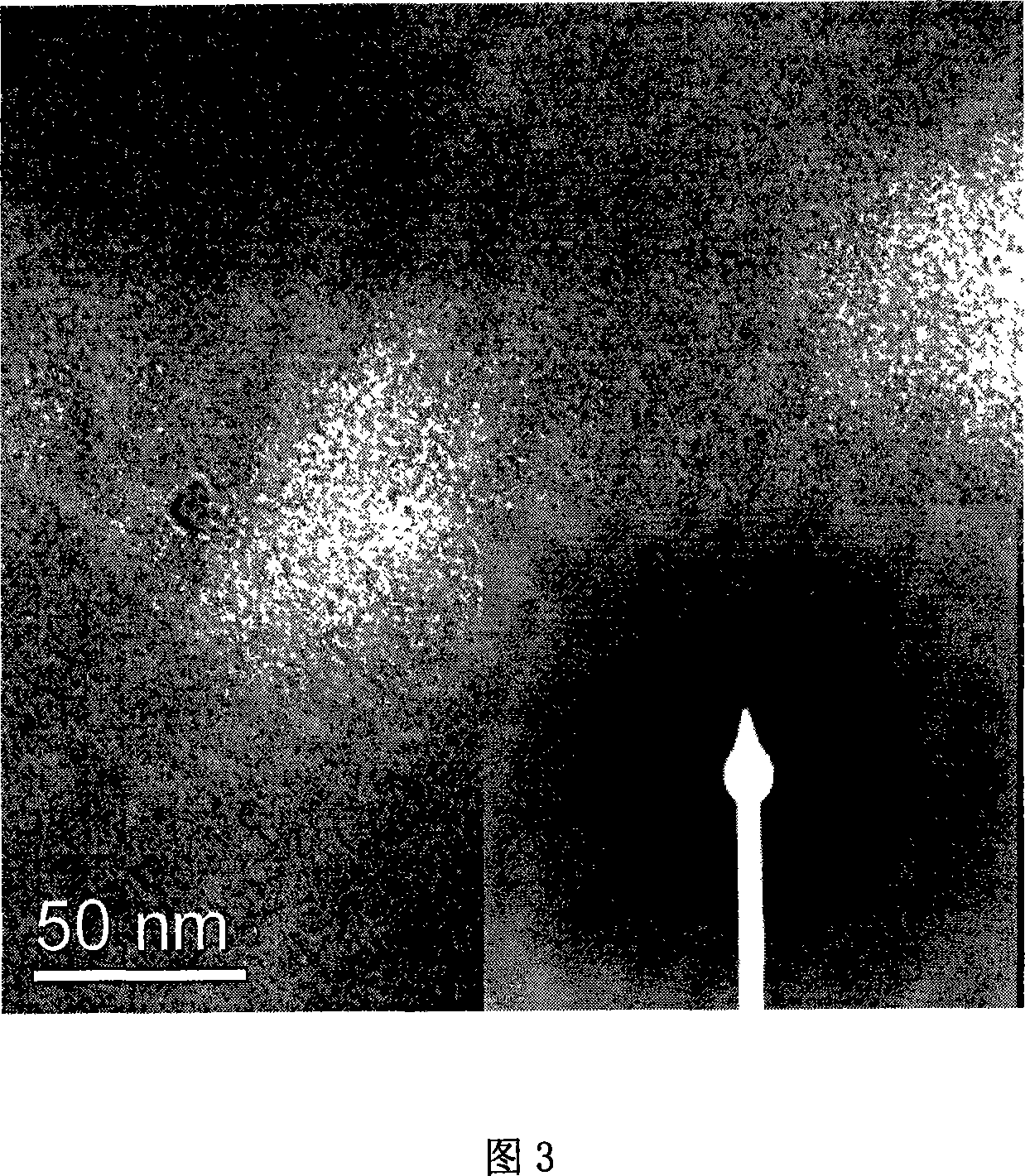
[0061] (1) AGS alloy target (9) is made by adopting suspension smelting cold crucible equipment: the ratio of Ag, Ge, Se mixture is 33% mol Ag, 20% molGe and 47% mol Se, and the melting ratio is good at 600°C. Form an alloy with a mixture of Ge, then continue to melt the silver-germanium alloy and Se at 500°C to form a block, and grind and cut the obtained block into a circular target.
[0062] (2) Fix the AGS target (9) on the target table (10) of the pulsed laser deposition film-making system, the substrate (6) is fixed on the substrate table (13), and the resistance heating furnace (15) is placed on the substrate Below the platform (13), they are all placed in the growth chamber (11) of the pulsed laser deposition film making system;
[0063] (3) growth chamber (11) is ev...
Embodiment 2
[0067] Embodiment 2. The preparation method of the non-volatile phase-change memory device based on solid electrolyte amorphous AGS thin film, its preparation steps are as follows:
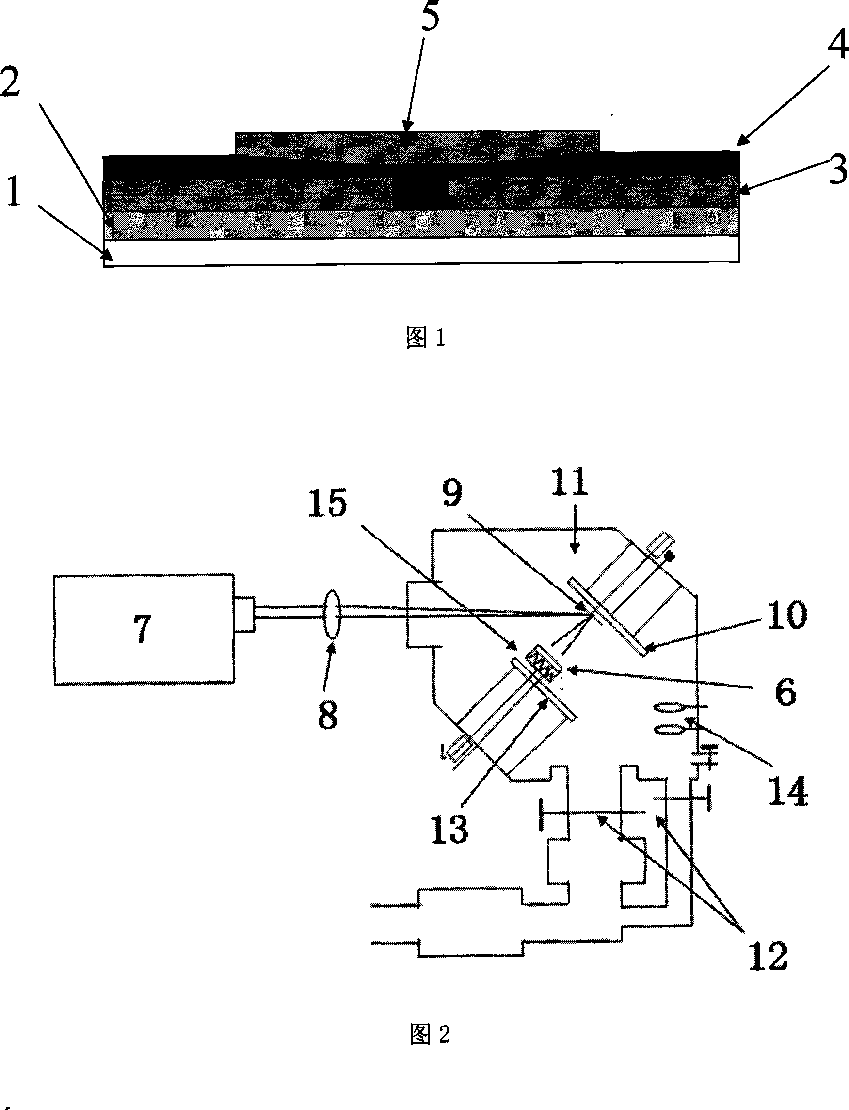
[0068] (1), deposit non-reactive electrode film 2 with pulsed laser deposition method on silicon chip substrate 1, its material is platinum, and the thickness of non-reactive electrode film 2 is 200 nanometers;
[0069] (2), utilize radio frequency magnetron sputtering method to deposit one deck insulating layer 3 on non-reactive electrode film 2, the material of insulating layer is silicon dioxide, and its thickness is 100 nanometers;
[0070] (3), utilizing the focused particle beam etching method in the insulating layer 2 to process micropores with a diameter of 100 nanometers, exposing the non-reactive electrode film 2 at the bottom;
[0071] (4) Cover the substrate with the microholes 5 with a metal mask that is engraved with a hole with a diameter of 0.5 mm, and align the holes of the mask w...
Embodiment 3
[0076] Embodiment 3. A method for preparing a non-volatile phase-change memory device based on a solid electrolyte amorphous AGS thin film. The specific preparation steps are as follows:
[0077] (1), utilize the radio frequency magnetron sputtering method to deposit one deck insulating layer 2 on the highly conductive silicon substrate 2, the material of insulating layer is silicon dioxide, and its thickness is 200 nanometers, uses silicon dioxide ceramic target during sputtering , using argon with a pressure of 10Pa as the sputtering gas, and a minimum lining temperature of 80°C;
[0078] (2), utilizing the focused ion beam etching method to process micropores with a diameter of 1 micron in the insulating layer 3, exposing the lower highly conductive silicon non-reactive electrode 2;
[0079] (3) Cover the substrate with the micro-holes processed with a metal mask with a hole of 0.4 mm in diameter, and align the holes of the mask with the micro-holes 5;
[0080] (4), put th...
PUM
| Property | Measurement | Unit |
|---|---|---|
| Thickness | aaaaa | aaaaa |
| Thickness | aaaaa | aaaaa |
Abstract
Description
Claims
Application Information