Metal-oxide-semiconductor transistor and method of manufacturing the same

An oxide semiconductor and manufacturing method technology, applied in semiconductor/solid-state device manufacturing, semiconductor devices, electrical components, etc., can solve the problems of the gate structure surface being easily exposed, affecting the performance of process reliability components, and improving reliability. performance, and the effect of improving component performance

Active Publication Date: 2008-02-27
UNITED MICROELECTRONICS CORP
View PDF0 Cites 6 Cited by
  • Summary
  • Abstract
  • Description
  • Claims
  • Application Information

AI Technical Summary

Problems solved by technology

[0005] However, part of the hard mask covering the gate structure will be removed during the etching process for forming spacers and trenches, removing the patterned photoresist layer in the photolithography process, and the pre-cleaning process. layer, making the surface of the gate structure easily exposed
Therefore, when a doped epitaxial layer is formed in the trench in the subsequent epitaxial process, an epitaxial layer, that is, a so-called polysilicon bump, will be formed on the surface of the exposed gate structure, which seriously affects the reliability of the process. and component performance

Method used


Image

  • Metal-oxide-semiconductor transistor and method of manufacturing the same
  • Metal-oxide-semiconductor transistor and method of manufacturing the same
  • Metal-oxide-semiconductor transistor and method of manufacturing the same

Examples


Embodiment Construction

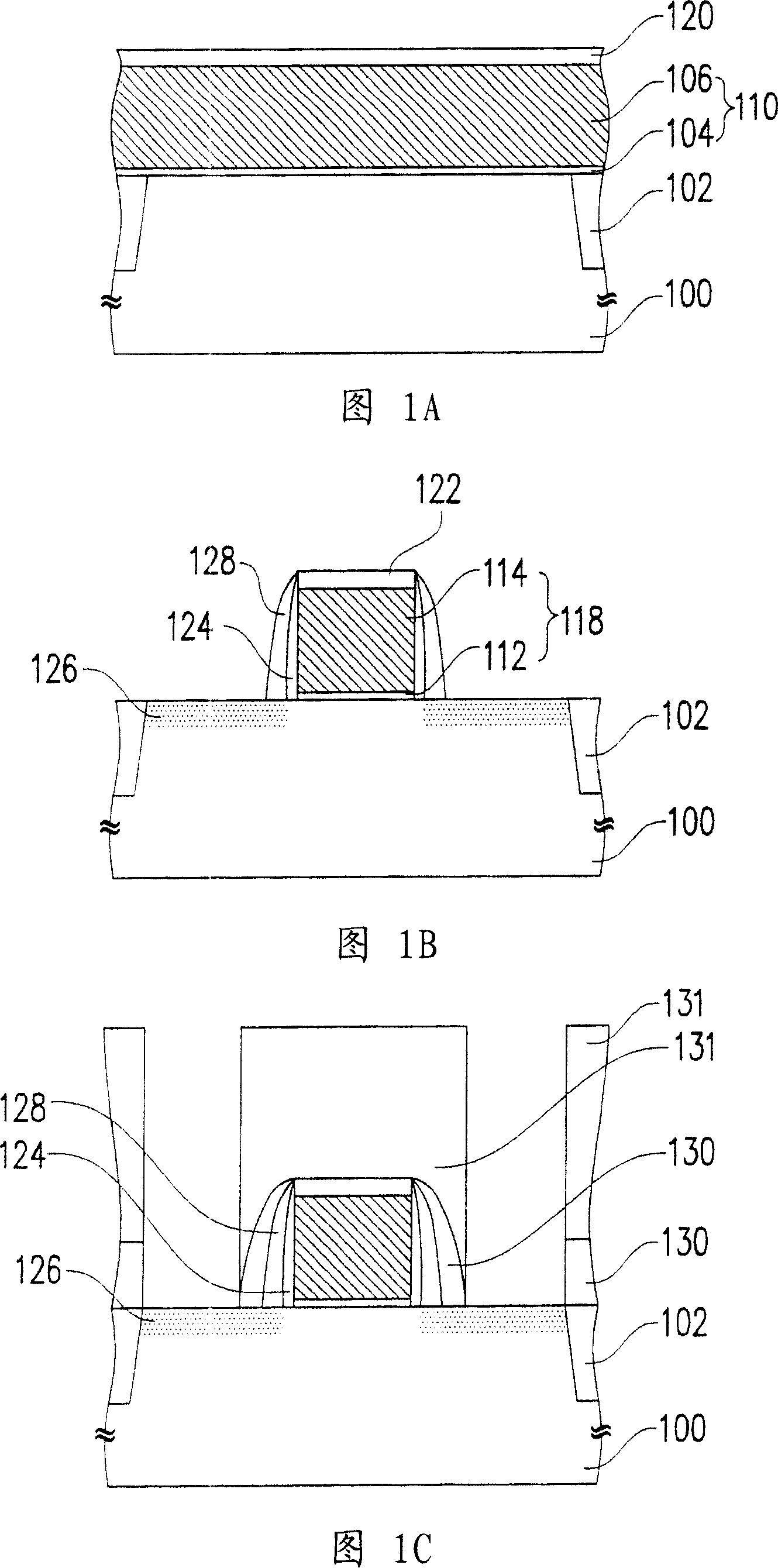
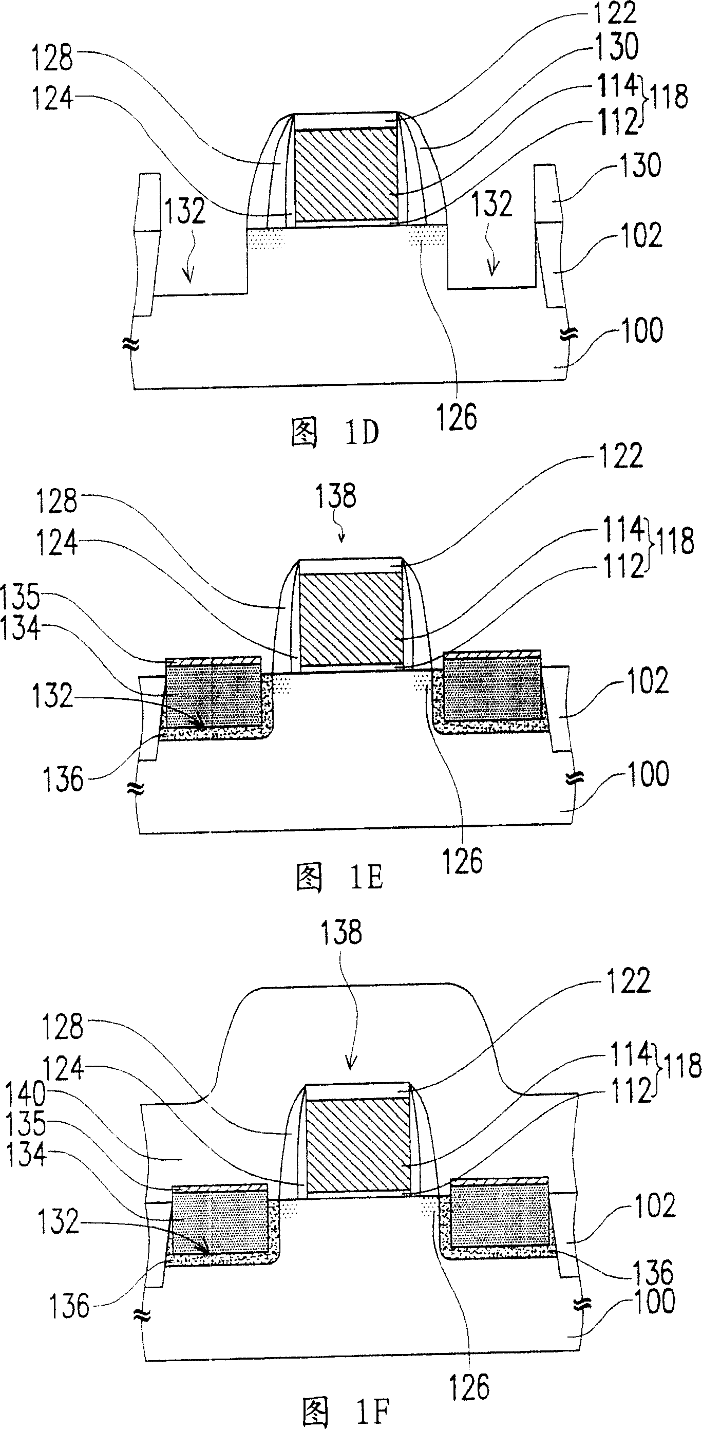
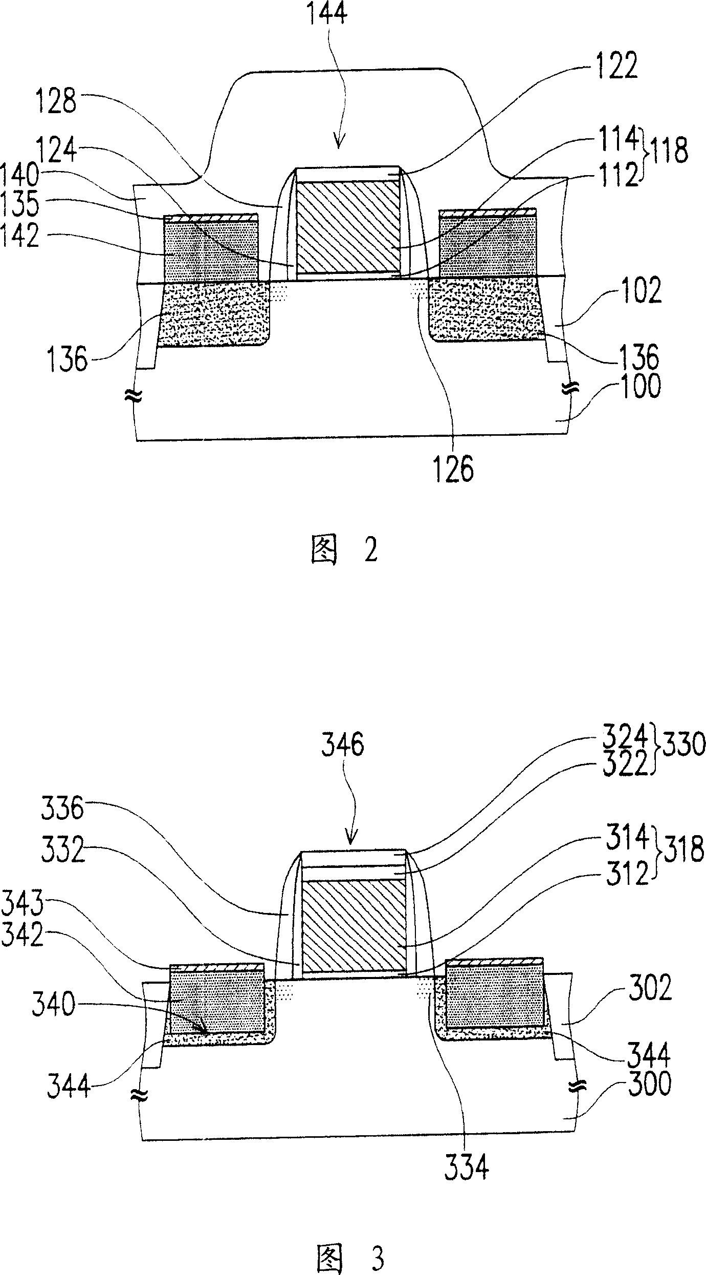
[0059] FIG. 1A to FIG. 1F illustrate a fabrication method of a metal oxide semiconductor transistor according to an embodiment of the present invention.

[0060] First, please refer to FIG. 1A , a substrate 100 on which a shallow trench isolation structure 102 has been formed is provided. The substrate 100 is, for example, a bulk silicon substrate. In another embodiment, the substrate 100 may also be a silicon-on-insulator substrate. Then, a gate structure material layer 110 is formed on the substrate 100 , and the gate structure material layer 110 includes a gate dielectric material layer 104 and a gate material layer 106 . The material of the gate dielectric material layer 104 is, for example, silicon oxide, silicon nitride, silicon oxynitride or high dielectric constant (K>4) material. The material of the gate material layer 106 is, for example, doped polysilicon. A method for forming the gate dielectric material layer 104 is, for example, a thermal oxidation method, and...


PUM


Abstract

The invention discloses a manufacturing method of metal oxide semiconductor transistors. This method includes following steps. It first provides a basement. Then, the material layer with the gate structure is formed on the basement. Later, the carbon-containing precursor gas and the reaction gas are pumped to form the carbon-containing mask material layer on the material layer with gate structure. Then, both carbon-containing mask material layer and the gate structure material layer are graphically modeled to form carbon-containing hard mask layer and gate structure. After that, the clearance wall is formed on the side wall of the gate structure and carbon-containing hard mask layer. Subsequently, the protective layer is formed on the basement. Then, some protective layer is removed to expose part of the surface of the substrate. Then, doping epitaxial layer is formed on the exposed surface of the basement formed.

Description

technical field [0001] The invention relates to a semiconductor element and a manufacturing method thereof, in particular to a metal oxide semiconductor transistor and a manufacturing method thereof. Background technique [0002] Metal-oxide-semiconductor transistors are extremely important components in VLSI circuits at present, and their applications are very wide, such as microprocessors, semiconductor storage elements, power elements, etc., can be used as metal-oxide-semiconductor transistors basic building block. [0003] In a general nanoscale process, in order to increase the device performance of metal oxide semiconductor transistors, trenches are first formed in the substrate on both sides of the gate structure, and then the epitaxial process will produce strained semiconductor materials (such as SiGe, SiC ) is filled in the trench as a source / drain region to increase the mobility of electrons or holes in the channel. [0004] The current method of applying strain...

Claims


Application Information

Patent Timeline
Patent Type & Authority Applications(China)
IPC IPC(8): H01L21/336H01L29/78
Inventor 郑博伦刘哲宏
Owner UNITED MICROELECTRONICS CORP
Why Eureka
Try Eureka