Alignment mark and its imaging optical system and imaging method

An alignment mark and optical system technology, applied in the field of optical systems, can solve the problems of reduced diffraction efficiency, attenuation of quasi-signal intensity, and impact on alignment accuracy, so as to increase the capture range, reduce the impact on alignment accuracy, and improve The effect of alignment accuracy

Active Publication Date: 2008-03-26
SHANGHAI MICRO ELECTRONICS EQUIP (GRP) CO LTD
View PDF1 Cites 18 Cited by
  • Summary
  • Abstract
  • Description
  • Claims
  • Application Information

AI Technical Summary

Problems solved by technology

The system uses a single blazed grating optimized at the center wavelength to separate polychromatic light, which will reduce the diffraction

Method used


Image

  • Alignment mark and its imaging optical system and imaging method
  • Alignment mark and its imaging optical system and imaging method
  • Alignment mark and its imaging optical system and imaging method

Examples


Embodiment Construction

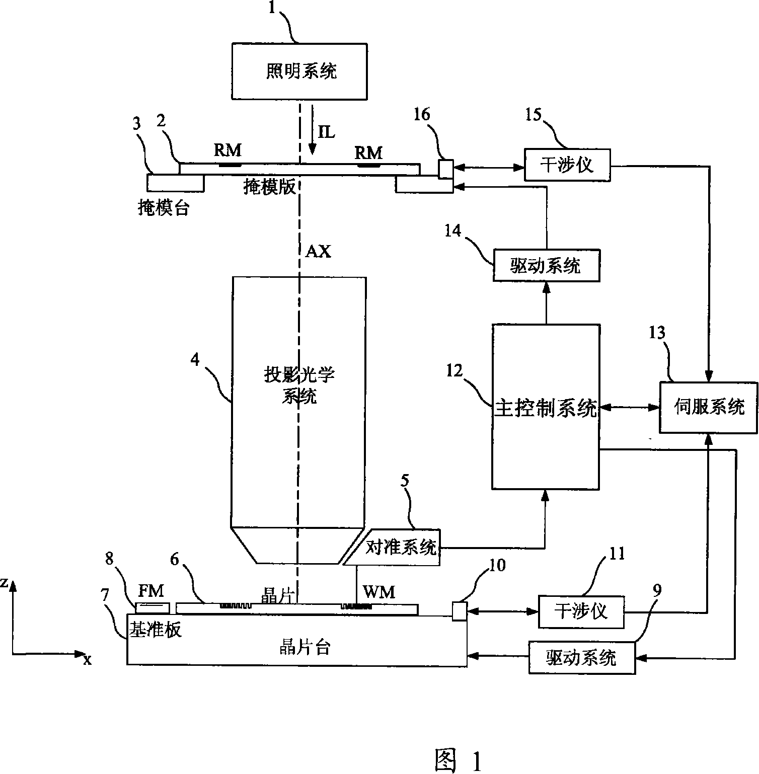
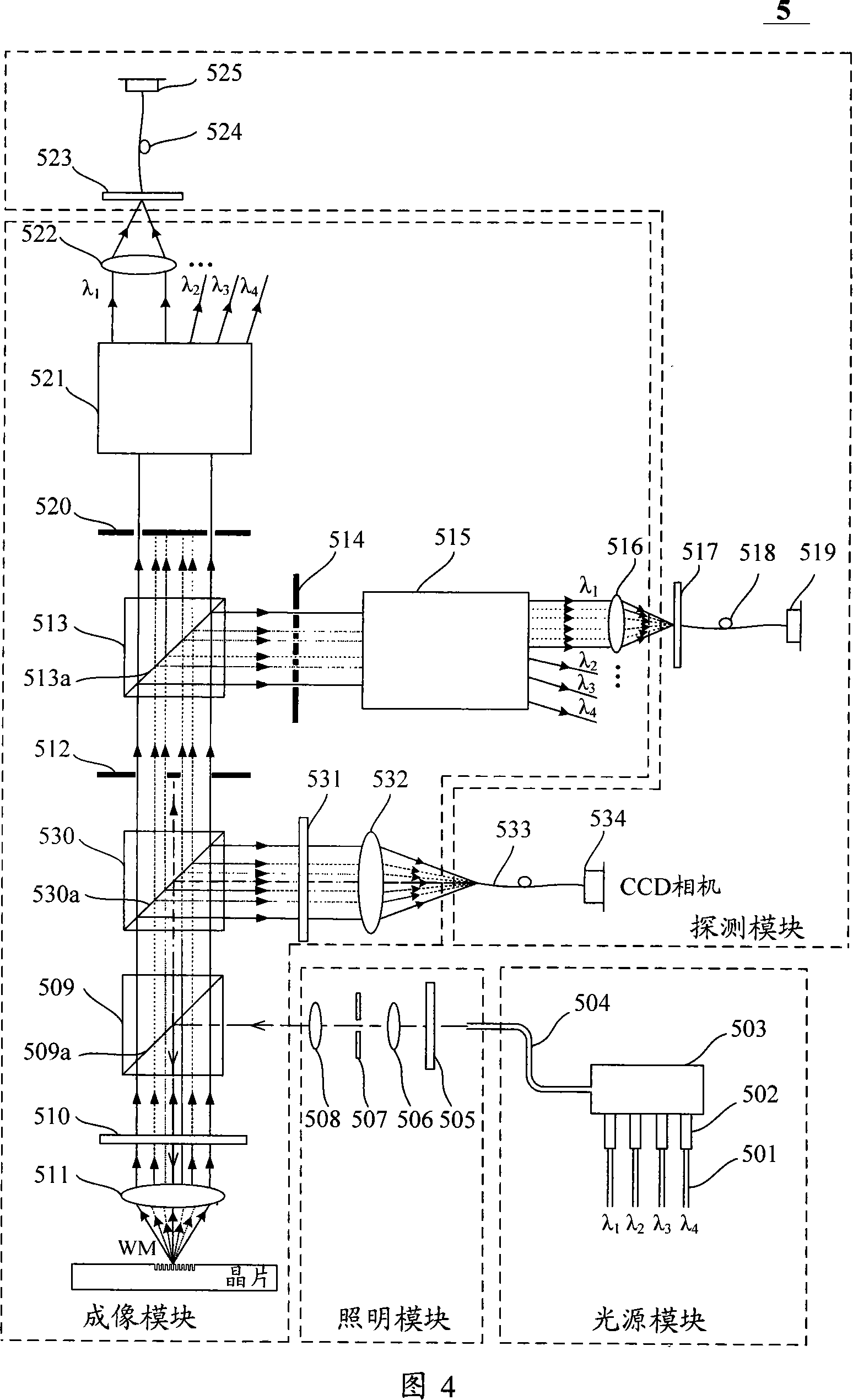
[0051] FIG. 1 is a schematic structural diagram of the alignment system of the lithography apparatus of the present invention and the overall layout and working principle between the alignment system and the existing lithography apparatus. As shown in Figure 1, the composition of the lithography apparatus includes: an illumination system 1 for providing exposure beams, an alignment mark RM reticle 2 provided with a mask pattern and a periodic structure, a mask for supporting the reticle 2 A mold stage 3, a wafer 6 provided with alignment marks WM of a periodic optical structure, a wafer stage 7 for supporting the wafer 6, and a projection optical system 4 for projecting the mask pattern on the reticle 2 onto the wafer 6 . On the wafer stage 7, there is a reference plate 8 engraved with a reference mark FM. In addition, the lithography apparatus includes an off-axis alignment system 5 for mask and wafer alignment, mirrors 10, 16 and interferometers 11, 15 for measuring the pos...


PUM


Abstract

This invention relates to a sort of alignment mark, and this alignment mark is the multiply periodic grating configuration. It consists of several group of the different periodic grating. This invention also offers a sort of imaging optical system of this alignment mark, and the alignment mark from the picture by this optical system, and it consists of this cohere imaging system at least. The first imaging system consists of frontal group lens, the first space wave filter, and the first back group lens. The second consists of the frontal group lens, the second space wave filter, and the second back group lens. This invention also offers a sort of the method which adopts this optical system to produce the picture to the alignment mark. This method consists of this approach: Offer and transfer the laser illuminating beam of light, and irradiate it to the alignment mark. Adopt the diffraction light and the reflex of the alignment mark. The diffraction light produces the picture by the first coheres imaging system and the second cohere imaging system of the optical system. This invention advances the detecting precision of the alignment mark availably.

Description

technical field [0001] The present invention relates to a lithography device in the field of integrated circuit IC or other micro device manufacturing, and relates to an alignment mark, an optical system for imaging the alignment mark and an imaging method. Background technique [0002] The photolithography apparatus in the prior art is mainly used in the manufacture of integrated circuits (ICs) or other micro devices. With a photolithographic apparatus, multilayer masks with different mask patterns are sequentially imaged in precise alignment on a photoresist-coated wafer, such as a semiconductor wafer or an LCD panel. Lithography devices are generally divided into two categories, one is a stepping lithography device, the mask pattern is exposed and imaged on one exposure area of ​​the wafer, and then the wafer moves relative to the mask to move the next exposure area to the mask pattern and under the projection objective, the mask pattern is again exposed on another expos...

Claims


Application Information

Patent Timeline
IPC IPC(8): G03F7/20G03F9/00H01L23/544
Inventor 徐荣伟韦学志李运锋周畅李铁军
Owner SHANGHAI MICRO ELECTRONICS EQUIP (GRP) CO LTD
Why Eureka
Try Eureka