

Xenon difluoride selective erosion for titanium nitride
A technology of xenon difluoride and titanium nitride, applied in gaseous chemical plating, chemical instruments and methods, cleaning methods and utensils, etc., can solve the problems of removing TiN deposition products and unusability
- Summary
- Abstract
- Description
- Claims
- Application Information
AI Technical Summary
Problems solved by technology
Method used
Image

Examples
Embodiment 1
[0036] XeF at various temperatures and pressures 2 Effectiveness of Etching Deposited Materials
[0037] In this example, XeF 2 Determined as etchant for TiN, SiO at various temperatures and pressures 2 and SiN etch rate. Coated with TiN, SiO 2 and SiN thin film silicon wafers to prepare test samples. The etch rate was calculated from the thickness change between the film's initial film thickness and its thickness after a period of exposure to etching or processing conditions.
[0038] In order to achieve etching, a large amount of XeF 2 Gases are introduced into the reaction chamber from gas cylinders through a virgin plasma generator. Once the desired pressure is reached, deactivate the XeF in the reaction chamber by shutting off the gas flow from the cylinder 2 The air pressure remains constant.
[0039] The test coupons were placed on a pedestal heater, which was used to maintain different substrate temperatures. The results are described in Table 1 below.
[004...
Embodiment 2
[0045] Via Xe and NF 3 The reaction forms XeF in situ 2
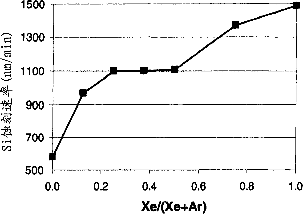
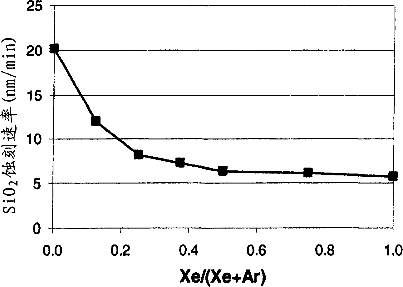
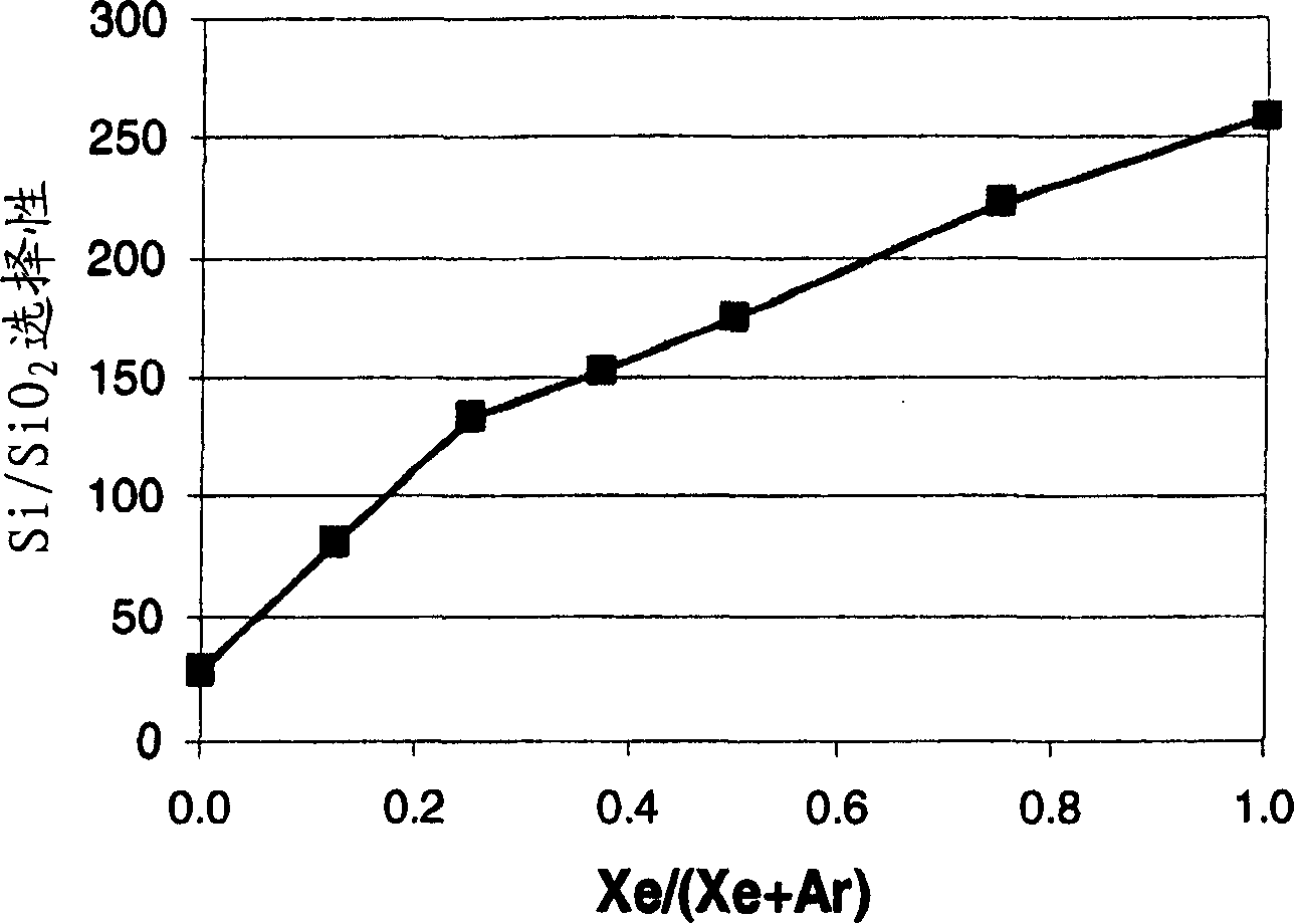
[0046] In this example, a MKS Astron remote plasma generator is installed in the upper part of the reaction chamber. The distance between the outlet of the Astron generator and the sample is approximately 6 inches. Start the remote plasma generator, but turn off the pedestal heater in the reactor. Keep the reaction chamber at room temperature. Measuring Si and SiO with Remote Plasma 2 The etch rate of the substrate is used for comparison.
[0047] The process gas added to the remote plasma is NF 3 , which is mixed with the second air stream in various amounts. The second gas flow includes Xe or argon (Ar) or a combination thereof. The total gas flow rate to the reaction chamber was fixed at 400 sccm, NF 3 The flow rate was fixed at 80 sccm. Although the total flow rate of the second gas stream was maintained at 320 sccm, the ratio of the flow rate of Xe to the total flow rate of the second gas stream (Xe / (Ar+X...
Embodiment 3
[0052] Remote plasma and temperature on TiN and SiO 2 The effect of etch rate
[0053] In this example the procedure of Example 2 was followed, except that both the remote plasma generator and the pedestal heater were turned on, so that the TiN and SiO 2 the etching rate.
[0054] In the first set of experiments, using NF 3 and Xe as a process gas for measuring TiN and SiO 2 the etching rate. The flow rate of Xe is fixed at 320 sccm. The temperature range is 100°C-150°C. TiN and SiO 2 The test results are as Figure 4 and Figure 5 Indicated by the square points in .
[0055] In the second set of experiments, using NF 3 Mixture with argon (Ar) as process gas for measurement of TiN and SiO 2 the etching rate. The flow rate of Ar was fixed at 320 sccm. The temperature range is 100°C-150°C. TiN and SiO 2 The test results are as Figure 4 and Figure 5 Shown by the diamond points in .
[0056] Such as Figure 4 It was shown that the addition of Xe to the process...
PUM
 Abstract
Description
Claims
Application Information