Watt level full solid state ultraviolet laser cleaning machine and laser cleaning method

A UV laser and laser cleaning technology, applied in cleaning methods and appliances, cleaning methods using gas flow, chemical instruments and methods, etc., can solve problems such as BBO crystal damage, application restrictions, photorefractive damage, etc., and achieve repetition rate High, low maintenance cost, small geometry effect

Inactive Publication Date: 2008-07-16
TSINGHUA UNIV +2
View PDF0 Cites 26 Cited by
  • Summary
  • Abstract
  • Description
  • Claims
  • Application Information

AI Technical Summary

Problems solved by technology

However, because BBO crystals are prone to photorefractive damage under ultraviolet laser irradiation, if the average power of the 266nm laser output after quadruple frequency exceeds 300mW, the BBO crystal will be destroyed
Since the output ultraviolet laser is below the watt level, the application of Nd:YAG and other all-solid-state lasers in the field of high-precision microelectronic substrate cleaning is greatly restricted.

Method used


Image

  • Watt level full solid state ultraviolet laser cleaning machine and laser cleaning method
  • Watt level full solid state ultraviolet laser cleaning machine and laser cleaning method

Examples


Embodiment 1

[0029] Using CLBO as a quadrupled Nd:YAG all-solid-state laser to output 1W 266nm laser, the pulse repetition frequency is 20.3Hz, and the spot diameter is 0.8cm to clean two thousand pieces of MH06LED substrates; the cleaning conditions are: constant temperature and humidity environment ( 25°C, 65%), Class 10,000 clean room, cleaning time for each component is 1.2 seconds. On the cleaned substrate, the LED chips are solidified and gold wire balls are soldered. Compared with the substrate without laser cleaning, the shear strength of the welded LED chips after cleaning is increased by 80%, the welding tension is increased by 120%, and the product yield is higher by 38%.

Embodiment 2

[0031] The Nd:YAG all-solid-state laser that uses CLBO as a quadruple frequency output 1W 266nm laser, the pulse repetition frequency is 20.3Hz, and the spot diameter is 0.8cm. It is used for the aluminum-based PCB board used in the LED backlight module for 26" liquid crystal displays. , cleaning treatment before electronic components welding, mainly cleaning the gold-plated pads on the aluminum-based PCB board, each PCB board has about 2000 pads. The cleaning conditions are: constant temperature and humidity environment (25°C, 65%), Class 10,000 clean room, cleaning time for each pad is 1.5 seconds. Use the cleaned PCB board for reflow soldering process, and solder the LED light source and related functional components on the PCB board. Compared with the PCB board without laser cleaning, The welding strength of the components welded after cleaning is greatly improved by about 80%, and the failure rate of component welding is reduced by about 90%, which reduces product repair l...

Embodiment 3

[0033] Using CLBO as a quadrupled Nd:YAG all-solid-state laser to output 1W 266nm laser, the pulse repetition frequency is 20.3Hz, and the spot diameter is 0.8cm. The ceramic substrate of the integrated package LED light source is cleaned. The ceramic substrate is AlN material. High thermal conductivity and silver plating on AlN for electrical pathways and pads. Clean the AlN plate with a laser before plating the silver layer. The cleaning conditions are: constant temperature and humidity environment (25°C, 65%), clean room with class 10,000, scan and clean the plate. Silver paste is plated on the cleaned AlN plate. Compared with the plate without laser cleaning, the adhesion of the plated silver layer after cleaning is increased by 120%, and there is little warping and peeling of the plated layer, and the product yield is higher by more than 40%.


PUM


Abstract

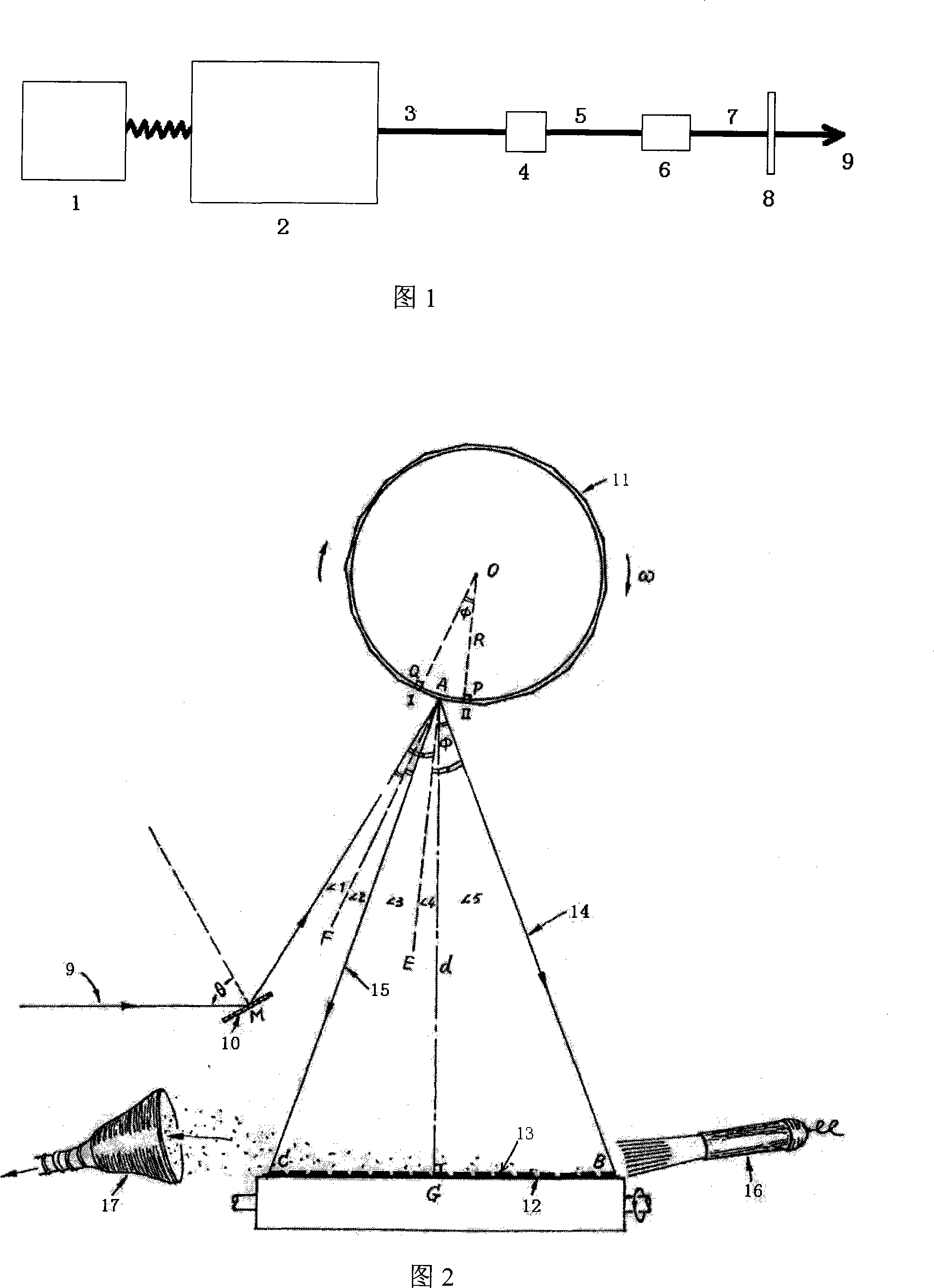
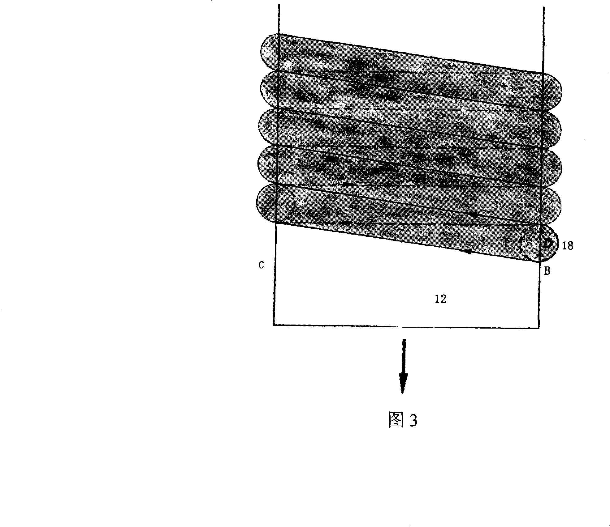
The invention discloses a Watt-level all-solid ultraviolet laser cleaner and a laser cleaning method, which pertains to the optical energy cleaning technology field and are applied to cleaning micro electronic substrate such as the integrated circuit. The power of the cleaner is connected with a laser resonance chamber; two non-linear optical crystals, a selective microscope and a reflector are positioned in the light path of pulsed laser from the laser resonance chamber; a rotating mirror drum is fixed above one side of the reflector; a work piece to be cleaned is arranged on a convey belt; a blower is positioned at one side of the convey belt and a cleaner is arranged at the other side. By adopting the method, substrates to be cleaned can be continuously or discontinuously conveyed to go through the laser which is Watt-level pulse laser with about 266nm and comes from the all-solid laser; proper laser intensity, pulse frequency and irradiation time can be controlled to effectively remove micron and submicron particles, organics, oily contamination, etc. on the surface of the substrate. The adhesion of the coating after cleaning and the product yield rate are greatly improved and the warp or spalling of the coating rarely happens.

Description

technical field [0001] The invention belongs to the scope of light energy cleaning equipment, in particular to a tile-level all-solid-state ultraviolet laser cleaning machine and a laser cleaning method. Background technique [0002] The technology of cleaning pollutants with laser was created in the mid-1970s, but it was not really applied in industrial production until the early 1990s. This is because with the rapid development of the microelectronics industry, the integration of integrated circuits, especially large-scale and ultra-large-scale integrated circuits, is getting higher and higher, and the cleanliness requirements for microelectronic substrates such as silicon wafers are also getting higher and higher. . Traditional cleaning techniques, such as mechanical cleaning, wet chemical cleaning, ultrasonic cleaning, etc. are often powerless to remove micron and submicron pollution particles. In addition, the mechanical removal method is easy to cause damage to the s...

Claims


Application Information

Patent Timeline
Patent Type & Authority Applications(China)
IPC IPC(8): B08B7/00B08B7/04B08B5/00
Inventor 沈德忠许祖彦李明远王桂玲沈光球王晓青
Owner TSINGHUA UNIV
Why Eureka
Try Eureka