Integrated opto-electronic device for generating high-frequency microwave by SOA four-wave mixing effect

An optoelectronic device, four-wave mixing technology, applied in the direction of electro-solid devices, laser parts, lasers, etc., can solve the problems of large and complex systems, poor stability, high cost, high integration, low cost and high yield Effect

Inactive Publication Date: 2008-07-16
TSINGHUA UNIV
View PDF0 Cites 32 Cited by
  • Summary
  • Abstract
  • Description
  • Claims
  • Application Information

AI Technical Summary

Problems solved by technology

As we all know, the systems built by discrete devices are often large and complex, with poor stability and relatively high cost.

Method used


Image

  • Integrated opto-electronic device for generating high-frequency microwave by SOA four-wave mixing effect
  • Integrated opto-electronic device for generating high-frequency microwave by SOA four-wave mixing effect

Examples


Embodiment 1

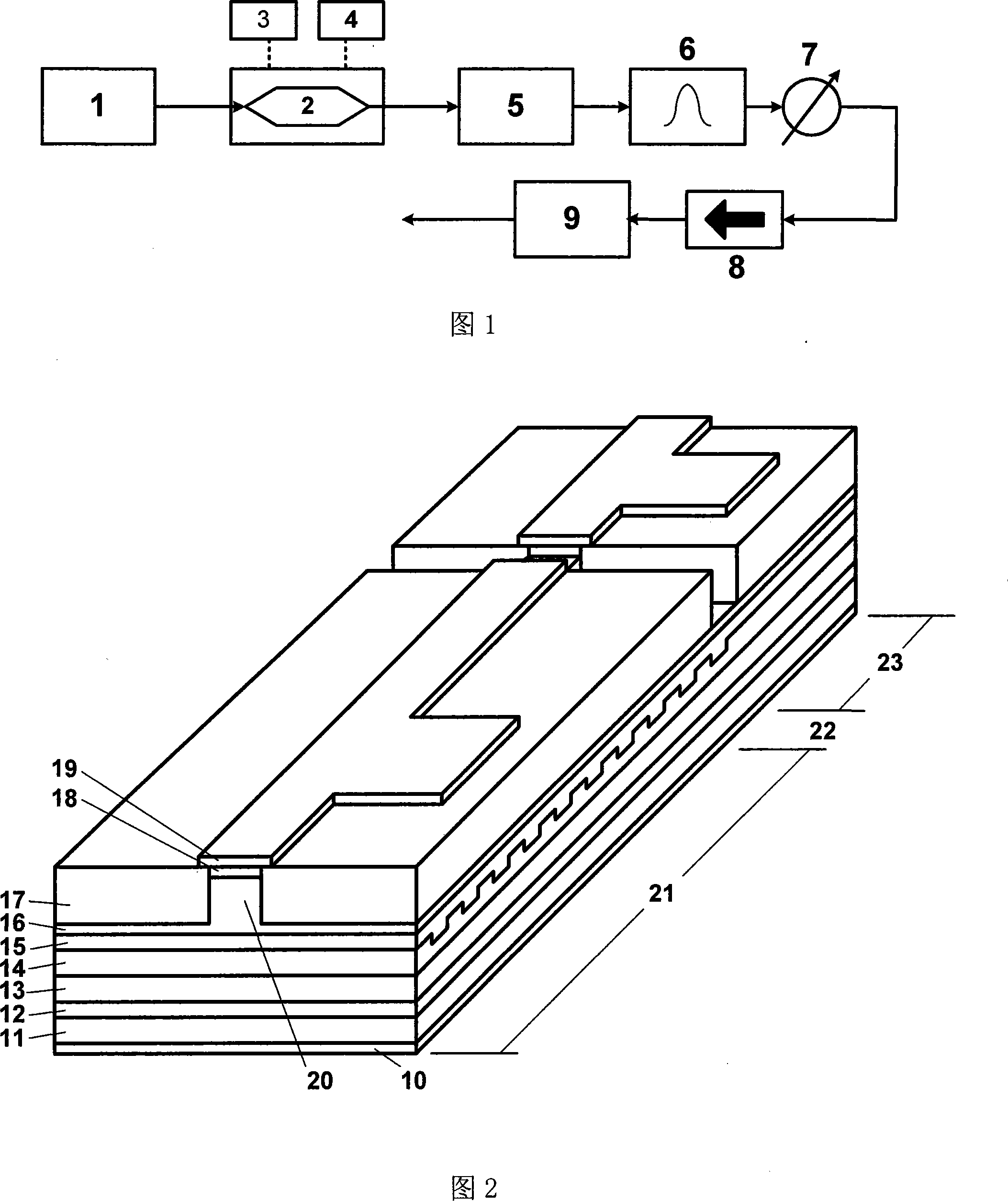
[0025]Referring to Figure 2, the working wavelength is in the 1550nm band, on the basis of direct modulation of DFB laser, using SOA four-wave mixing effect to generate high-frequency microwave InGaAsP / InP-based monolithic photonic integrated device.

[0026] The device integrates a DFB laser 21 and an SOA 23 on the same chip.

[0027] First, the epitaxial materials of the device are as follows. Through the MOCVD method, first epitaxially grow on the n-type substrate material once, and then grow the n-type InP lower cladding layer 11 (thickness 200nm, doping concentration about 1×10 18 cm -2 ), 100nm thick undoped lattice-matched InGaAsP waveguide layer 12 (photoluminescence wavelength 1.2μm), strained InGaAsP multiple quantum wells 13 (photoluminescence wavelength 1.52μm, 7 quantum wells: well width 8nm, 0.5% compressive strain, barrier InGaAsP grating material layer 14 with a width of 10 nm, a lattice matching material, and a photoluminescent wavelength of 1.2 μm) and a th...

Embodiment 2

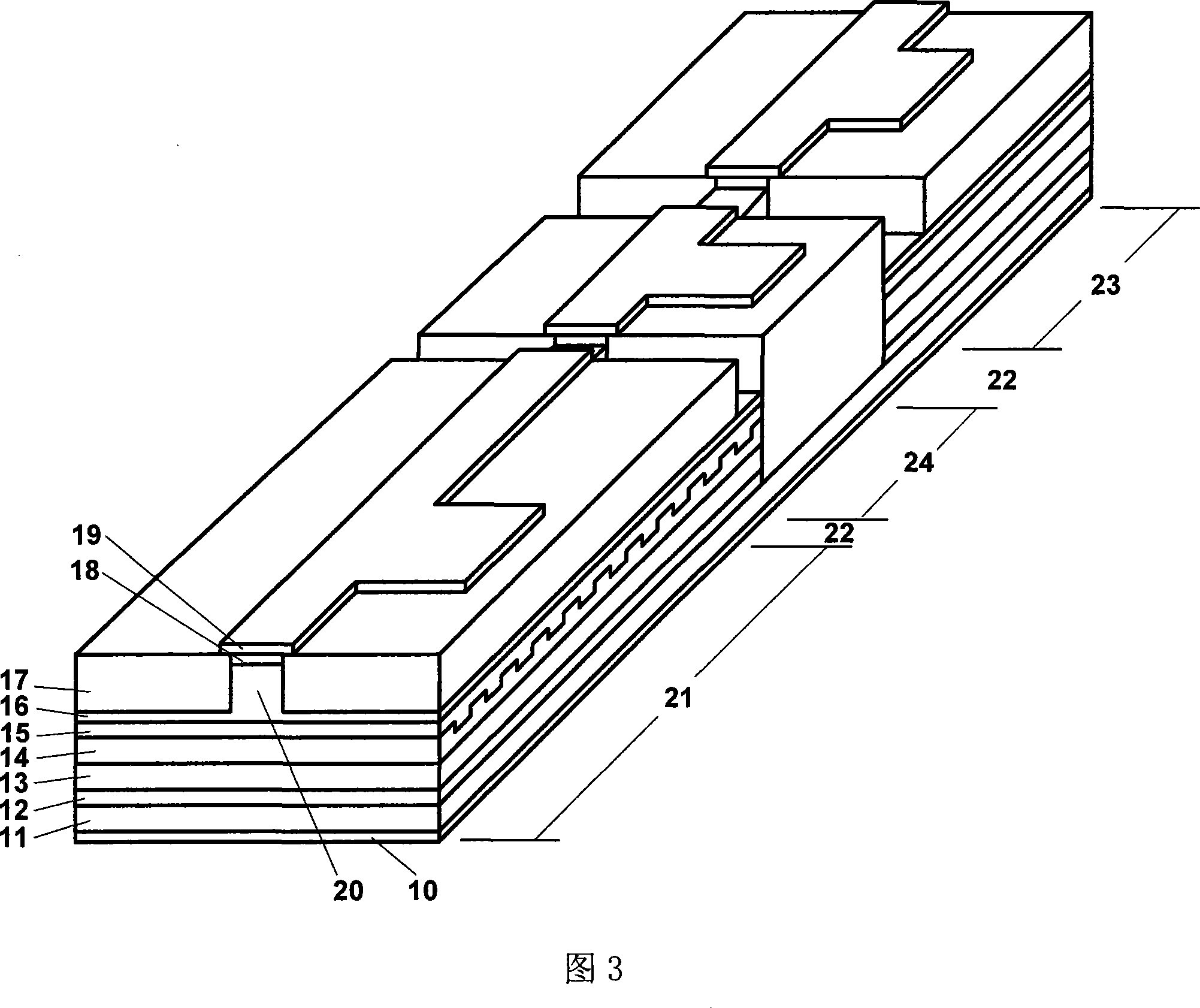
[0031] Referring to Figure 3, the working wavelength is in the 1550nm band, on the basis of indirect modulation of DFB lasers, using the SOA four-wave mixing effect to generate high-frequency microwave InGaAsP / InP-based monolithic photonic integrated devices.

[0032] The device integrates a DFB laser 21, an EA modulator 24 and an SOA 23 on the same chip.

[0033] First, the epitaxial materials of the device are as follows. Through the MOCVD method, first epitaxially grow on the n-type substrate material once, and then grow the n-type InP lower cladding layer 11 (thickness 200nm, doping concentration about 1×10 18 cm -2 ), 100nm thick undoped lattice-matched InGaAsP waveguide layer 12 (photoluminescence wavelength 1.2μm), strained InGaAsP multiple quantum wells 13 (photoluminescence wavelength 1.52μm, 7 quantum wells: well width 8nm, 0.5% compressive strain, barrier InGaAsP grating material layer 14 with a width of 10 nm, a lattice matching material, and a photoluminescent w...


PUM

PropertyMeasurementUnit
Lengthaaaaaaaaaa
Lengthaaaaaaaaaa
Lengthaaaaaaaaaa

Abstract

The invention belongs to the photoelectronic device technical field, in particular relating to an integrated photoelectronic device which utilizes SOA four-wave mixing effect to generate high-frequency microwaves. The integrated photoelectronic device has a ridged waveguide structure; two sides of a ridged waveguide are filled with and leveled up with SiO2 insulating layers, and integrates a distributed feedback DFB laser and a semiconductor optical amplifier SOA. The top and the bottom of the DFB laser and the SOA are respectively provided with a layer of P type electrode and a layer of N type electrode, the connection part of the DFB laser and the SOA is provided with a section of electrical isolation section on which the layer of P type electrode and an ohmic contact layer do not exist. Two one-order modulation sidebands generated by output light of the DFB laser are taken as pump light of SOA four-wave mixing effect to generate two light with larger frequency differences to perform heterodyne. The device has the advantages of high integration level, low cost, high rate of finished products, simple production method and improvement of performance.

Description

technical field [0001] The invention belongs to the technical field of optoelectronic devices, and in particular relates to an integrated optoelectronic device for generating high-frequency microwaves by using the SOA four-wave mixing effect. Background technique [0002] The invention is a monolithic photonic integrated device based on the four-wave mixing effect of a semiconductor optical amplifier (Semiconductor Optical Amplifier, SOA), which generates high-frequency microwaves through optical heterodyne, and has a wide range of applications, including wireless local area networks, antenna remote control etc. The following first briefly introduces the importance of high-frequency microwave or millimeter wave in wireless communication, and then introduces the application of optoelectronic technology in millimeter wave wireless communication. [0003] In recent years, with the continuous development of optical fiber networks and the Internet (Internet), voice, image, data,...

Claims


Application Information

Patent Timeline
IPC IPC(8): H01S5/50H01S5/34H01S5/22H01S5/026H01S1/02H01L27/15
Inventor 孙长征黄缙熊兵罗毅
Owner TSINGHUA UNIV
Why Eureka
Try Eureka