Active part array base plate and LCD panel
A technology for liquid crystal display panels and array substrates, which is applied to electrical components, semiconductor devices, electrical solid devices, etc., can solve the problems of covering the conductive layer, the film thickness of the electrode layer is too thin, and the display abnormality of the liquid crystal display panel. The effect of avoiding corrosion
- Summary
- Abstract
- Description
- Claims
- Application Information
AI Technical Summary
Problems solved by technology
Method used
Image

Examples
no. 1 example
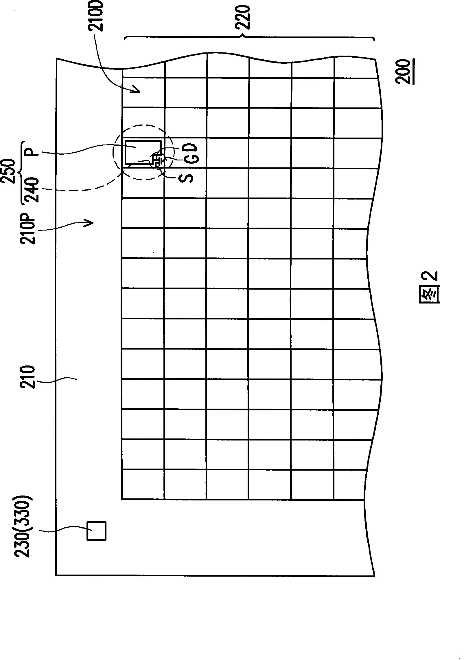
[0060] FIG. 2 is a schematic diagram of the active device array substrate in the first embodiment of the present invention. Referring to FIG. 2 , the active device array substrate 200 includes a substrate 210 , a pixel array 220 and at least one bonding pad 230 . Wherein, the substrate 210 has a display area 210D and a peripheral circuit area 210P adjacent to the display area 210D, and the peripheral circuit area 210P substantially surrounds the display area 210D. The pixel array 220 is disposed on the substrate 210 and located in the display area 210D, and the bonding pad 230 is disposed on the substrate 210 and located in the peripheral circuit area 210P. In addition, in this embodiment, the pixel array 220 is composed of, for example, a plurality of pixel units 250, wherein each pixel unit 250 includes a thin film transistor 240 and a pixel electrode P, and the thin film transistor 240 has a gate G, a source S and a drain d. The pixel electrode P is disposed on part of th...
no. 2 example
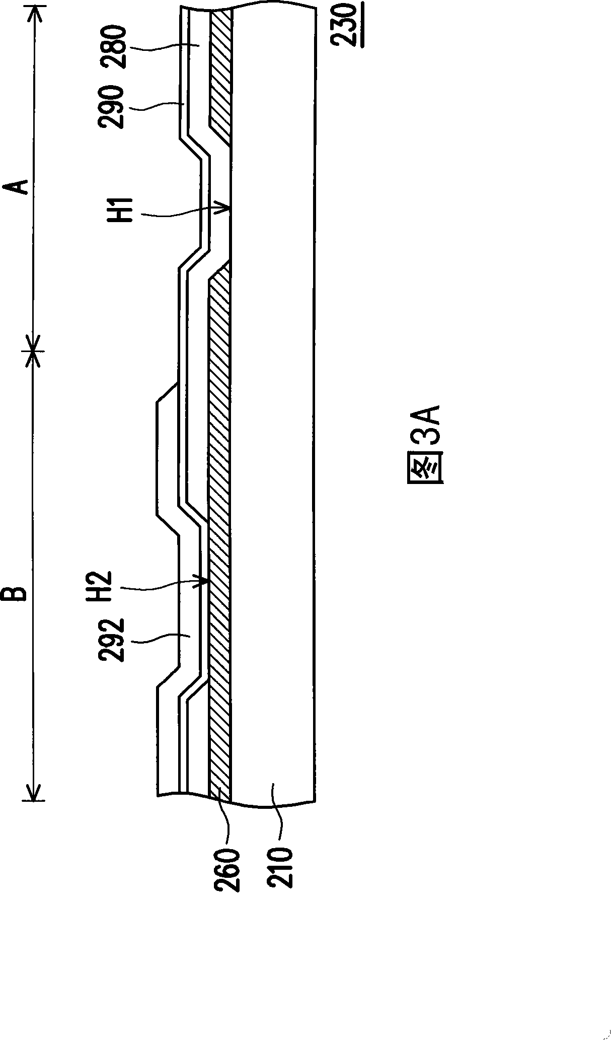
[0065] 3B is a schematic cross-sectional view of another bonding pad and a pixel unit in the second embodiment of the present invention. Please refer to FIG. 3B, the bonding pad 330 is similar to the bonding pad 230 in FIG. The second conductive layer 270, so that the electrode layer 290 is connected to the first conductive layer 260 through the second conductive layer 270 in the interlayer conductive region B. Specifically, the material of the second conductive layer 270 can be aluminum, molybdenum, titanium, neodymium, a laminate thereof, or an alloy thereof, and the second conductive layer 270 can further reduce the gap between the first conductive layer 260 and the electrode layer 290. The contact resistance value (contact resistance), and then enhance the signal transmission effect between the film layers in the interlayer conduction region B.
[0066] In fact, the fabrication of the film layer of the bonding pad 230 can be completed when the pixel array 220 is fabricate...
no. 3 example
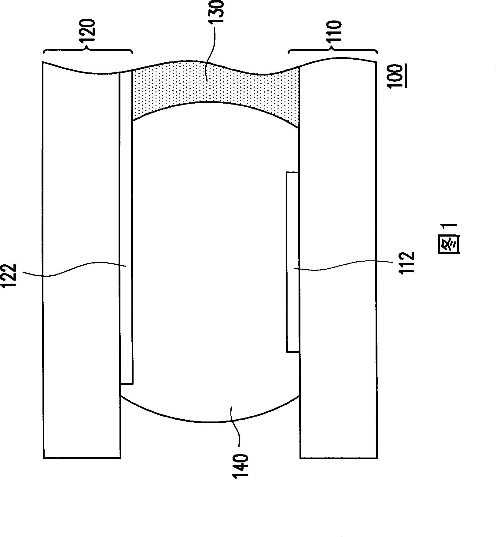
[0071] FIG. 5 is a schematic cross-sectional view of a liquid crystal display panel according to a third embodiment of the present invention. Please refer to FIG. 5, the liquid crystal display panel 400 includes an active element array substrate 410, an opposite substrate 420, a plastic frame 430, and a liquid crystal layer 440, wherein the active element array substrate 410 is, for example, a bonding pad 450 having any of the above-mentioned embodiments. The active device array substrate 410, wherein the bonding pads 450 are, for example, the bonding pads 230, 330 in the above-mentioned embodiments. The opposite substrate 420 is disposed on the opposite side of the active device array substrate 410 and has a common electrode 422 . In addition, the plastic frame 430 is located between the common electrode 422 and the active device array substrate 410 , and the liquid crystal layer 440 is disposed in a space surrounded by the active device array substrate 410 , the opposite sub...
PUM
 Abstract
Description
Claims
Application Information
 - R&D
- Intellectual Property
- Life Sciences
- Materials
- Tech Scout
- Unparalleled Data Quality
- Higher Quality Content
- 60% Fewer Hallucinations
Browse by: Latest US Patents, China's latest patents, Technical Efficacy Thesaurus, Application Domain, Technology Topic, Popular Technical Reports.
© 2025 PatSnap. All rights reserved.Legal|Privacy policy|Modern Slavery Act Transparency Statement|Sitemap|About US| Contact US: help@patsnap.com