Method for intensifying light absorption of thin-film solar cell

A thin film and performance technology, applied in the field of solar photovoltaic equipment, can solve the problems of poor controllability and repeatability of roughness, increased absorption of incident light, poor electrical conductivity, etc.

Inactive Publication Date: 2008-08-20
BEIJING XINGZHE MULTIMEDIA TECH
View PDF0 Cites 29 Cited by
  • Summary
  • Abstract
  • Description
  • Claims
  • Application Information

AI Technical Summary

Problems solved by technology

[0004] The commonly used front electrode TCO, such as tin oxide, is difficult to make with a high degree of surface texture or roughness when its thickness does not exceed 1000 nm, that is, its ability to scatter light is often unsatisfactory
TCOs with rough surfaces often have poor electrical conductivity and high light loss, which limits the further improvement of the photoelectric efficiency of thin-film photovoltaic devices
There have been various attempts to make the surface texture of TCO more obvious, such as chemically or mechanically treating the deposited TCO film to make the surface rougher, but the roughness obtained by this method is not as good as Very good control and repeatability, which often leads to defects in thin-film photovoltaic devices
Another approach is to increase the thickness of the TCO, so that its surface roughness increases with the thickness, but the thickened TCO increases its absorption of incident light, and also prolongs the production cycle of photovoltaic devices.

Method used


Image

  • Method for intensifying light absorption of thin-film solar cell
  • Method for intensifying light absorption of thin-film solar cell

Examples


Embodiment Construction

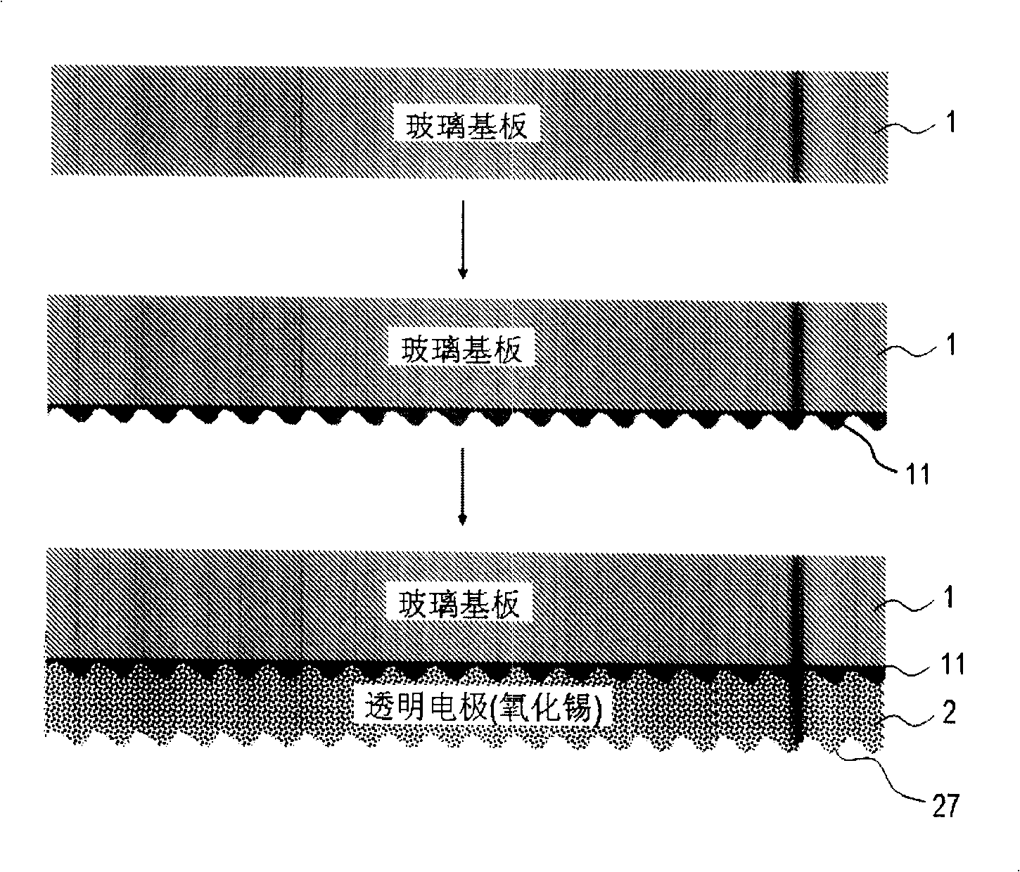
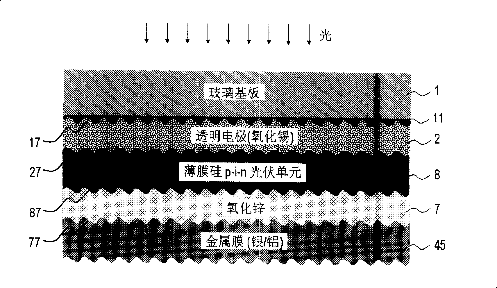
[0013] Such as figure 1 As shown, the first step of the present invention is to clean the flat glass plate 1, and then use sol-gel deposition method (sol-gel) to coat glass balls on the surface of the glass substrate. The specific method is to immerse the glass plate in a sol containing glass beads and adhesives, and constantly stir the sol or move the substrate itself, so that the glass beads evenly adhere to the surface of the glass substrate, and then the glass The substrate is taken out from the sol stagnant body, and heat-treated at a temperature not higher than 500° C. to solidify the adhesive, so that the glass beads are firmly attached to the glass substrate, forming a film layer 11 with an undulating structure. Thereafter, a transparent front electrode 2 (TCO), such as tin oxide or zinc oxide, is deposited on the surface layer 11 so that its surface 27 has a surface roughness similar to that of the glass surface layer 11 or to a greater extent. The average undulation...


PUM


Abstract

The present invention discloses a method for increasing light absorption of film solar cell. Firstly, depositing glass beards with diameter less than 1 mum on glass substrate to make the surface has fluctuation structure with propriety mum dimension. Then depositing transparent front electrode to make it has surface structure with evident light scattering effect. The film photovoltaic device formed on the transparent front electrode has higher light absorption capacity and conversion efficiency.

Description

technical field [0001] The invention belongs to the field of solar photovoltaic devices, in particular to the manufacturing technology of thin-film silicon-based photovoltaic devices. Background technique [0002] In recent years, the development of photovoltaic cells and large-area photovoltaic modules has attracted widespread attention in the world. Hydrogenated amorphous silicon and nanocrystalline silicon, in particular, have shown great potential with the widespread adoption of photovoltaic devices in commercial and residential installations. A notable feature of producing thin-film silicon photovoltaic devices at such a low temperature below 260°C is that the large-area deposited silicon-related semiconductor film layers and electrical contact film layers have excellent performance. At the same time, using well-established coating equipment and procedures, low-cost stencils can be produced industrially. The laser patterning of different thin films applied on the same...

Claims


Application Information

Patent Timeline
Patent Type & Authority Applications(China)
IPC IPC(8): H01L31/075H01L31/042H01L31/0236H01L31/0224H01L31/0445
CPCY02E10/548
Inventor 李沅民马昕
Owner BEIJING XINGZHE MULTIMEDIA TECH
Why Eureka
Try Eureka