Amorphous boron carbon alloy and photovoltaic application thereof

A boron carbon and amorphous technology, applied in the field of semiconductor material production, can solve the problems of not eliminating the n-p junction effect, difficulty in conductivity, and not being easily applied, and achieve the effect of improving photoelectric conversion performance and good compatibility

Inactive Publication Date: 2008-08-20
BEIJING XINGZHE MULTIMEDIA TECH
View PDF2 Cites 11 Cited by
  • Summary
  • Abstract
  • Description
  • Claims
  • Application Information

AI Technical Summary

Problems solved by technology

However, this method of fabricating tunnel junctions cannot be easily applied to the aforementioned multi-junction p-i-n devices because amorphous silicon cannot be easily doped to grow into highly conductive thin films
Wide bandgap alloys, such as amorphous silicon carbon (a-SiC) and amorphous silicon nitrogen (a-SiN), are the preferred materials for forming the p-layer or n-layer of amorphous silicon p-i-n photovoltaic devices. Due to the above advantages, they are used to Increased light transmission per photovoltaic cell in multijunction devices, but achieving sufficiently high electrical conductivity at the same time is especially difficult
Thus, attempts at p- or n-layers of amorphous silicon multi-junction p-i-n photovoltaic devices composed of highly doped, wide-bandgap alloys have not achieved satisfactory tunnel junctions, that is, have not eliminated The n-p junction effect that exists between

Method used


Image

  • Amorphous boron carbon alloy and photovoltaic application thereof
  • Amorphous boron carbon alloy and photovoltaic application thereof
  • Amorphous boron carbon alloy and photovoltaic application thereof

Examples


Embodiment 1

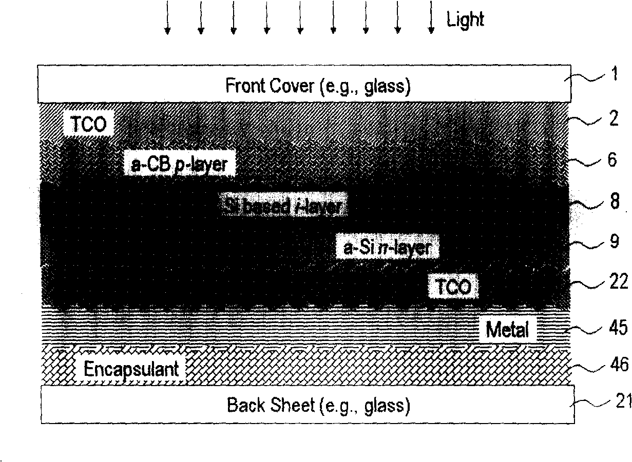
[0030] The p-layer has a significant impact on the conversion efficiency of p-i-n solar cells based on silicon thin films. The hydrogenated amorphous boron carbon film has an optical energy band gap greater than 2.0 eV, which can be used to replace the traditional wide band gap p-layer based on amorphous silicon (usually boron-doped amorphous silicon carbon, a-SiC) . For example Figure one In the pin-type photovoltaic cell shown, the p-layer 6 is composed of a hydrogenated amorphous boron carbon film with a thickness of no more than 15 nanometers and a light energy band gap of 2.0-2.2 eV, which is directly on the transparent conductive oxide front electrode 2. Generated by plasma coating method. The i-layer 8 may be based on an amorphous silicon film or a nano-silicon layer. The phosphorus-doped n-layer 9 is formed of ordinary amorphous silicon. The interface formed by the hydrogenated amorphous boron carbon p-layer 6 and the undoped intrinsic i-layer 8 is a unique heterojunction ...

Embodiment 2

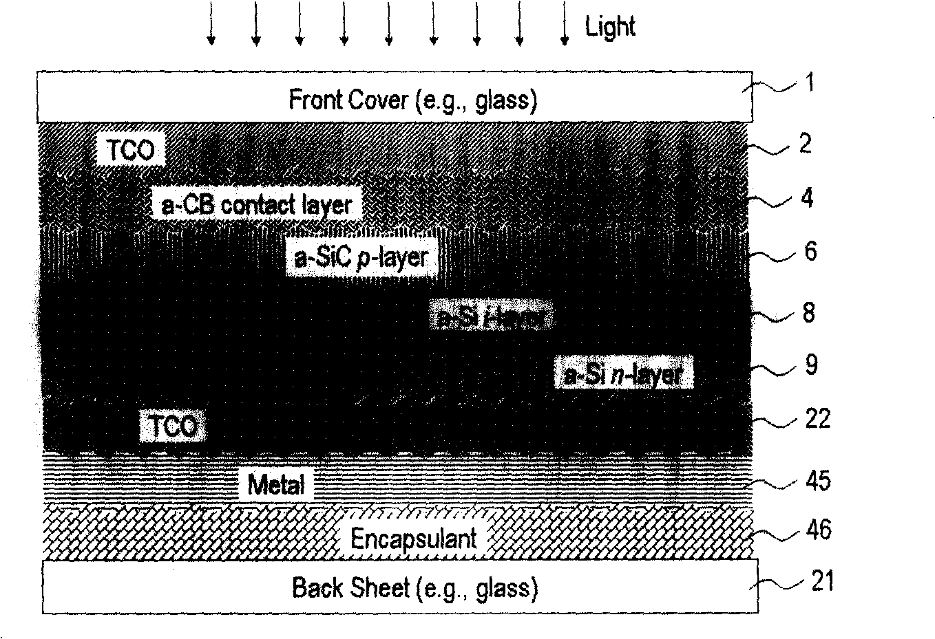
[0032] figure 2 In the single junction photovoltaic cell based on amorphous silicon, except that the p-layer 6 is composed of a conventional amorphous silicon-carbon alloy, it is basically the same as figure 1 The p-i-n device used in the first embodiment shown has the same structure. The difference and uniqueness is that it has a hydrogenated amorphous boron carbon contact layer 4, which is placed on the front electrode 2 and the hydrogenated amorphous silicon carbon p-layer 6. The function of the hydrogenated amorphous boron-carbon contact layer 4 is to reduce the resistance (electrical barrier) between the transparent conductive oxide and the amorphous silicon-carbon p-layer. Since a high concentration of carbon atoms must be used to minimize the amount of light loss and increase the light transmission rate as much as possible, the p-layer is almost completely electrically insulated. The ultra-thin hydrogenated amorphous boron carbon layer with a thickness of less than 3 nan...

Embodiment 3

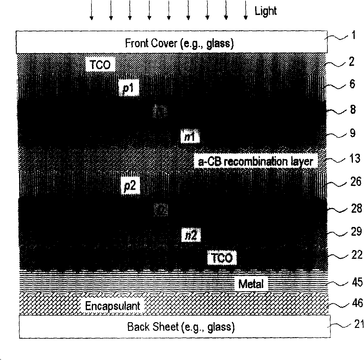
[0034] Multi-junction photovoltaic cells based on silicon thin films are composed of two or more p-i-n photovoltaic units connected with the same optical path and circuit, superimposed on top of each other. Each p-i-n photovoltaic unit is called a junction. The band gap widths of multiple i-layers based on silicon thin films in a multi-junction photovoltaic cell can be the same or different. In order to eliminate resistance or reverse n-p junctions between adjacent photovoltaic cells, multi-junction photovoltaic devices require a composite layer or tunnel junction. To image 3 The double-junction stacked photovoltaic device shown is taken as an example. Two photovoltaic units (top junction and bottom junction) are connected end to end and stacked on top of each other to form an integrated photovoltaic device. The top junction is composed of p1-i1-n1 (6-8-9), the bottom junction is composed of p2-i2-n2 (26-28-29), and there is a composite layer 13 between the two junctions. The othe...


PUM

PropertyMeasurementUnit
band gapaaaaaaaaaa
thicknessaaaaaaaaaa
thicknessaaaaaaaaaa

Abstract

The present invention discloses produce and application of hydrogenation amorphous boron carbon (a-CB) film. Amorphous boron carbon alloy can be formed at low temperature by plasma enhanced chemical vapor deposition method. The p type semiconductor film can be used to single junction and multi-junction photovoltaic devices and improves the capability of single junction and multi-junction photovoltaic devices.

Description

Technical field [0001] The invention belongs to the manufacturing range of semiconductor materials, and particularly relates to material technology applied to thin-film photovoltaic devices. Background technique [0002] In recent years, the development of thin-film solar photovoltaic cells and large-area modules or templates (photoelectric components) has attracted worldwide attention. The huge potential of hydrogenated amorphous silicon, especially nanocrystalline silicon (nano-silicon), which is widely used in commercial and residential optoelectronic devices, has been shown. An important feature of hydrogenated silicon thin film optoelectronic devices made at temperatures below 260°C is that when the semiconductor silicon thin film and electrical contact layer are deposited on a large area, inexpensive thin film substrate materials and sophisticated processing methods and equipment are used. , So that it has the advantages of low production cost and excellent performance at t...

Claims


Application Information

Patent Timeline
Patent Type & Authority Applications(China)
IPC IPC(8): H01L31/075H01L31/042H01L31/20H01L31/032H01L31/0445H01L31/046
CPCY02E10/548Y02P70/50
Inventor 李沅民马昕
Owner BEIJING XINGZHE MULTIMEDIA TECH
Why Eureka
Try Eureka