
Method of manufacturing semiconductor element

A manufacturing method and semiconductor technology, applied in the direction of semiconductor/solid-state device manufacturing, semiconductor devices, electrical components, etc., can solve problems such as device damage, and achieve the effect of preventing device failure and preventing device damage.

Active Publication Date: 2008-09-03
FUJI ELECTRIC CO LTD
View PDF5 Cites 22 Cited by
  • Summary
  • Abstract
  • Description
  • Claims
  • Application Information

AI Technical Summary

Problems solved by technology

This creates another problem - device damage

Method used


Image

  • Method of manufacturing semiconductor element
  • Method of manufacturing semiconductor element
  • Method of manufacturing semiconductor element

Examples


no. 1 approach

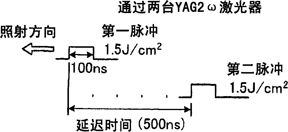
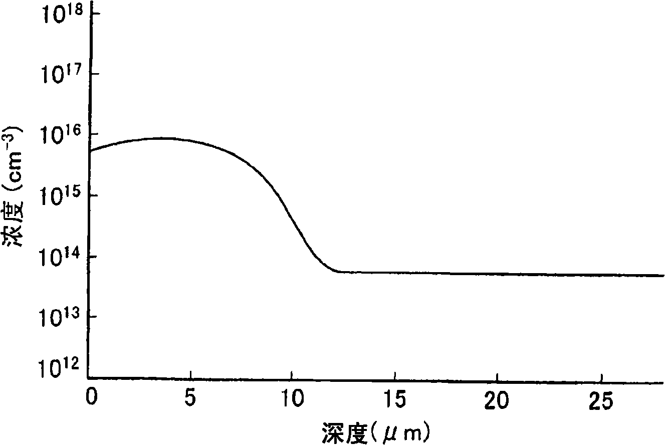
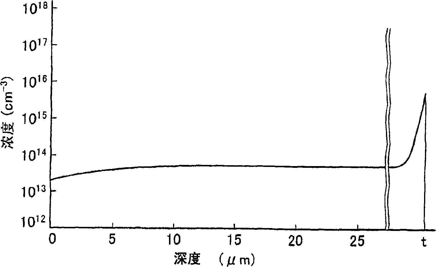
[0055] The first embodiment uses lithium as a dopant in the ion implantation step to form n + type layer 10a to form Figure 16 shown in the n-type buffer and p + type collector layer. After this ion implantation step, when n + type layer 10a and p + When the type layer 8a is activated and provides an upper surface contact layer in contact with the lower surface electrode, laser annealing is performed using two all-solid-state YAG2ω lasers (wavelength 532 nm) in the step of activating the upper surface contact layer.

[0056] figure 1 is showing the pulse shape of the pulsed laser beam emitted from each of the two laser emitting devices. Such as figure 1 As shown, when the laser beams are emitted, the full width at half maximum (corresponding to the pulse width) of the two lasers is, for example, 100 ns. Also, the energy density of each of the first laser beam (first pulse) and the second laser beam (second pulse) is, for example, 1.5 J / cm 2 , so that the total energ...

no. 2 approach

[0063] In Embodiment 2, a semiconductor laser (wavelength: 800 nm) is used instead of one of the two all-solid-state YAG2ω lasers (wavelength: 532 nm) in the first embodiment. Using lithium as a dopant to form n + type layer 10a.

[0064] Figure 5 is a view showing the pulse shape of a pulsed laser beam emitted from an all-solid-state YAG2ω laser and continuous oscillation of a semiconductor laser. Such as Figure 5 As shown, when the laser beam is emitted, the full width at half maximum (corresponding to the pulse width) of the laser emitted by the all-solid-state YAG2ω laser is, for example, 100 ns. Moreover, the irradiation energy density of the all-solid-state YAG2ω laser is, for example, 1.5J / cm 2 . During wafer processing, a laser beam is emitted from a semiconductor laser at, for example, 5J / cm 2 The energy density is irradiated on the entire wafer surface. Likewise, the pulse coverage ratio of an all-solid-state YAG2ω laser is, for example, 90%.

[0065] In or...


PUM


Abstract

The invention relates to a method of manufacturing a semiconductor element. In the implanting step, Li, S or Se ions as a dopant having a larger diffusion coefficient to silicon than P or As usually used as a dopant in silicon semiconductor manufacturing process. In the activating step, the ion implanted surface is laser annealed by combining a solid laser or an excimer laser and a semiconductor laser, the semiconductor laser irradiates the whole wafer surface with laser beams. The solid laser or excimer laser emits pulsed laser beams. Device failure of the manufactured semiconductor element is avoided by this arrangement, thus manufacturing a semiconductor element having satisfactory characteristics. Device breakage of the manufactured semiconductor element due to heat induced during laser irradiation is prevented by this method.

Description

technical field [0001] The present invention relates to a method of manufacturing a semiconductor element, and more particularly to a method of manufacturing semiconductor elements such as IC (Integrated Circuit), MOS (Metal Oxide Semiconductor), and Insulated Gate Bipolar Transistor (hereinafter referred to simply as IGBT) . Background technique [0002] In recent years, integrated circuits (ICs) have been widely used as important components of computers or communication equipment. In these ICs, a large number of transistors and resistors are connected to form an electronic circuit integrated on one chip. ICs including power semiconductor elements among these ICs are called power ICs. [0003] An IGBT is a power element that has both the high-speed switching and voltage-driven characteristics of a MOSFET and the low turn-on voltage of a bipolar transistor. IGBT components have expanded from industrial applications including devices such as general-purpose converters, AC ...

Claims


Application Information

Patent Timeline
Patent Type & Authority Applications(China)
IPC IPC(8): H01L21/04H01L21/324H01L21/265
CPCH01L21/268H01L21/26513H01L29/7395H01L29/66333H01L29/167H01L21/2658
Inventor 中泽治雄
Owner FUJI ELECTRIC CO LTD
Learn More