Metal semiconductor composite ultra-distinguish film and preparation method thereof

A metal-semiconductor, super-resolution technology, applied in the field of optical storage, can solve the problems of focusing spot energy attenuation, damage to the film and substrate, shortening the life of the disc, etc., to achieve high light energy utilization, simple preparation method, fast signal response Effect

Inactive Publication Date: 2008-09-10
SHANGHAI INST OF OPTICS & FINE MECHANICS CHINESE ACAD OF SCI
View PDF0 Cites 5 Cited by
  • Summary
  • Abstract
  • Description
  • Claims
  • Application Information

AI Technical Summary

Problems solved by technology

[0005] (1) While reducing the effective size of the focused spot, it will cause the attenuation of the energy of the focused spot. Therefore, a higher readout laser power is often required, which affects the life of the laser. At the same time, the high temperature in the irradiation will damage the film and substrate. disk, shorten the life of the disk;

Method used


Image

  • Metal semiconductor composite ultra-distinguish film and preparation method thereof

Examples


Example Embodiment

[0020] Example 1:

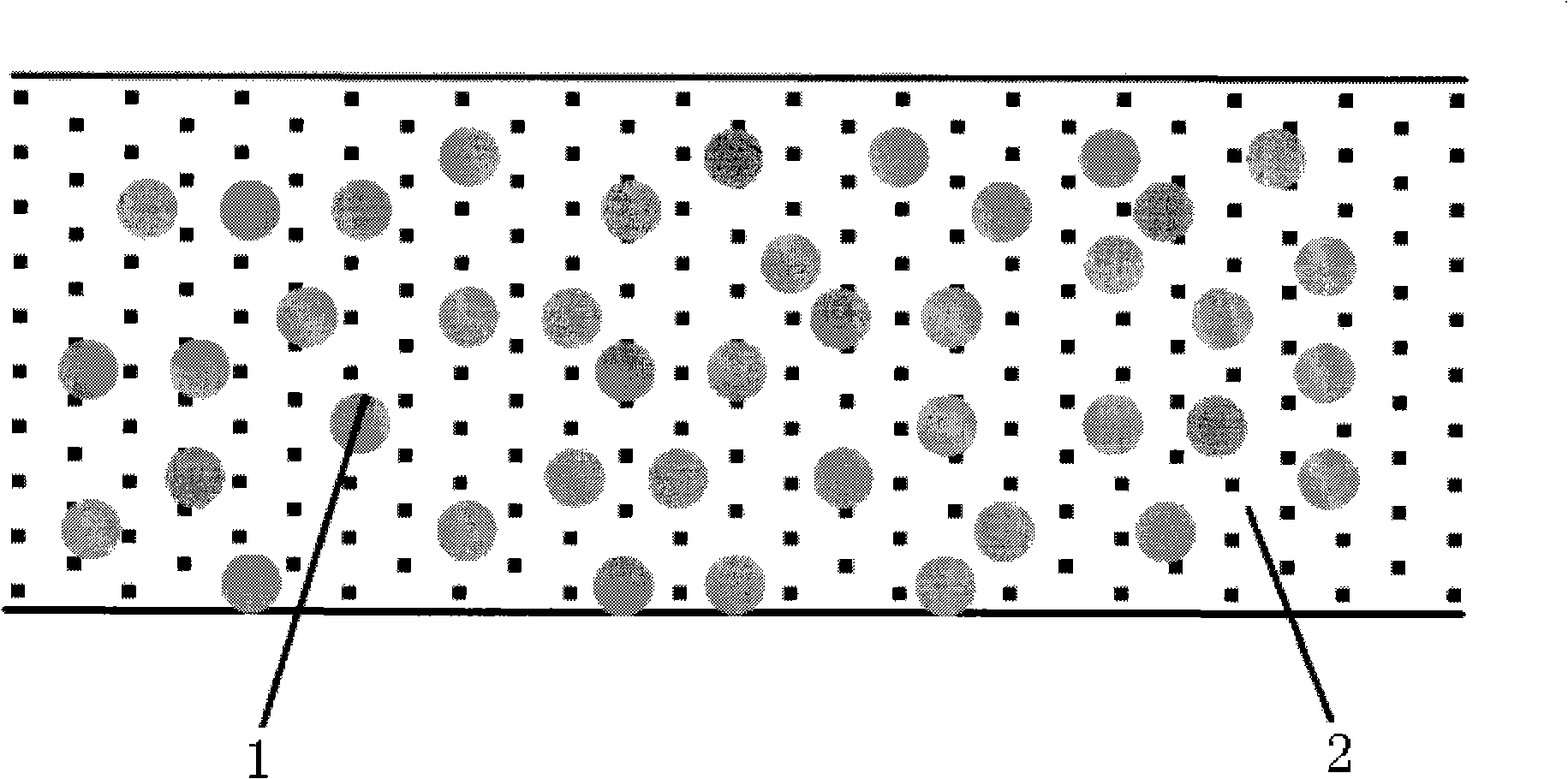
[0021] Taking the Ag-Si composite film as an example, a mixed target with a molar ratio of Ag and Si of 1:9 is used as the sputtering target. The substrate is a polycarbonate disc with a thickness of 1.2 mm. The engraved pit points are used as information points. Pump the background vacuum of the sputtering chamber to 6.0×10 -4 After Pa, argon gas is introduced, the flow rate of argon gas is 70 sccm, the sputtering pressure is adjusted to 0.6Pa, the sputtering power is 250W, and the composite target is pre-sputtered for 5 minutes to remove the pollution on the surface of the composite target, and then sputtered for 10 minutes , to obtain the desired Ag-Si composite film. figure 1 It is a structural schematic diagram of the metal-semiconductor composite thin film of this embodiment, and the thin film is composed of a semiconductor matrix 2 and nanometer metal (Ag or Au or Pt or Pd) particles 1 buried in it or located on its surface. In order to test its s...


PUM


Abstract

The invention relates to a metal semiconductor composite super resolution film and a preparation method thereof. The film is a metal semiconductor composite film formed by depositing metal argent, aurum, platinum or palladium and semiconductor on a substrate by a magnetron sputtering method; the film is provided with a nanometer microstructure formed by metal nanometer particles or clusters irregularly distributed on the semiconductor silicon substrate or the surface of the substrate; the components of the nanometer metal particles is argent, aurum, platinum or palladium; the dimension of the metal particles or clusters is 5 nm to 100 nm. The structure of the invention can make full use of plasma reinforcement effect on local surface produced by the metal particles and the optical nonlinear effect of the semiconductor silicon, read an information point less than an optical diffraction limit and achieve the effect of super resolution. In addition, the super resolution film for optical storage also has the advantages of simple preparation method, rapid response time, good read-out stability, strong signals, etc.

Description

technical field [0001] The invention relates to optical storage, in particular to a metal-semiconductor composite super-resolution film and a preparation method thereof which can reduce the read-write spot size on a recording layer and are applied to an optical disc. Background technique [0002] With the development of the information age, especially the development and popularization of digital high-definition film and television technology and network technology, CD memory is required to have higher storage density and capacity. The most direct way to increase storage density and capacity is to reduce the recording point size. However, the minimum recording point size depends on the optical resolution of the optical disc storage system. Therefore, people often increase the resolution of the optical system by reducing the laser wavelength and increasing the numerical aperture of the optical head objective lens. In the former case, due to the difficulty in developing short...

Claims


Application Information

Patent Timeline
IPC IPC(8): C23C14/35C23C14/14C23C14/54G11B7/26
Inventor 蒋志耿永友魏劲松
Owner SHANGHAI INST OF OPTICS & FINE MECHANICS CHINESE ACAD OF SCI
Why Eureka
Try Eureka