
Tantalum doping tin oxide thin film carrier material for gene chip

A carrier material, gene chip technology, applied in the direction of analyzing materials, material analysis by electromagnetic means, biochemical equipment and methods, etc., can solve the problem of poor stability of biological signal detection sensitivity chips, expensive biological signal detection equipment, and has not yet been found. Tantalum-doped tin oxide thin film and other problems, to achieve high sensitivity and strong specificity label-free electrical detection, easy industrial production, simple and easy preparation process

Inactive Publication Date: 2008-09-17
KUNMING UNIV OF SCI & TECH
View PDF0 Cites 4 Cited by
  • Summary
  • Abstract
  • Description
  • Claims
  • Application Information

AI Technical Summary

Problems solved by technology

However, despite the rapid development of gene chip technology for more than ten years, it still cannot become a technology that can be generally used in clinical medicine and experimental research, and it faces many key problems that need to be solved urgently.
[0003] At present, the most mature and widely used detection technology in gene chips is the fluorescent labeling method. The disadvantages of this method are: the target samples to be detected need to be labeled with fluorescein, the process is complicated and the technical cost is high; the detection equipment of biological signals (Gene chip scanner) is expensive and relatively large in size, making it difficult to achieve portability and miniaturization; biological signal detection sensitivity and chip stability are poor, etc.
Through the search of the prior art literature, no relevant reports have been found about the use of tantalum-doped tin oxide thin films as gene chip carrier materials

Method used


Image

  • Tantalum doping tin oxide thin film carrier material for gene chip
  • Tantalum doping tin oxide thin film carrier material for gene chip

Examples


Embodiment 1

[0034] (1) Ta with a purity of 99.99% 2 o 5 and SnO 2 The powder is fully mixed, pressed into a billet under a pressure of 80Mpa, put into a high-temperature sintering furnace and sintered at 1650°C for 3 hours to obtain a tantalum-doped tin oxide sputtering target, in which Ta 2 o5 The mass percentage (wt.%) is 1%, SnO 2 The mass percentage (wt.%) of the target is 99%, and the size of the target is 60mm in diameter and 6mm in thickness;

[0035] (2) The prepared tantalum-doped tin oxide sputtering target is fully cleaned with analytical pure acetone and deionized water, then placed in an oven, and kept at 120°C for 3 hours to remove surface oil and other impurities;

[0036] (3) Use ordinary slide glass as the film substrate material, fully wash it with analytical pure acetone and deionized water before sputtering, then put it in an oven, and keep it warm at 80°C for 2 hours;

[0037] (4) Install and put the target material and glass slide pretreated in (2) and (3) into t...

Embodiment 2

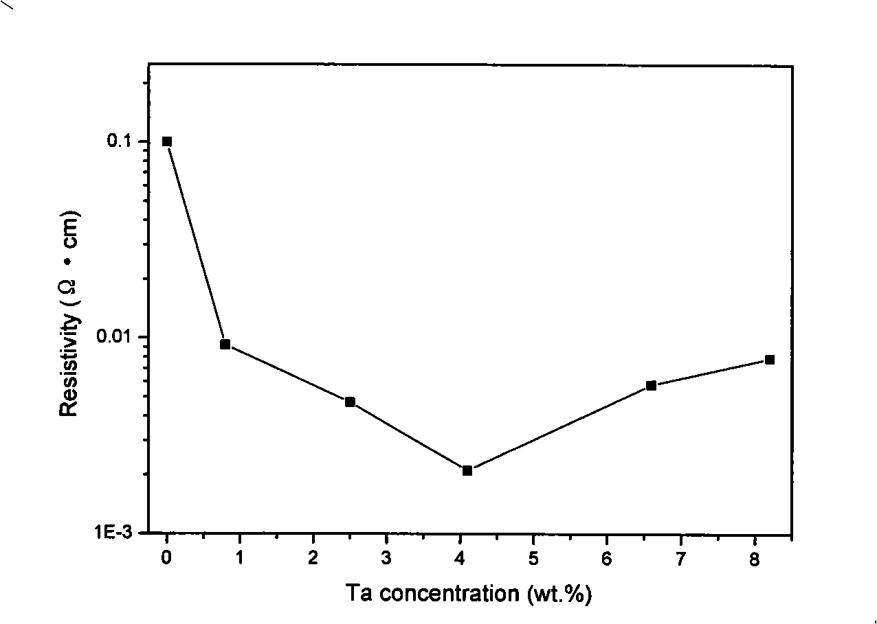
[0043] Except that the composition and preparation parameters of the sputtering target are different from those in Example 1: the Ta with a purity of 99.99% 2 o 5 and SnO 2 The powder is fully mixed, pressed into a billet under a pressure of 80Mpa, put into a high-temperature sintering furnace and sintered at 1600°C for 4 hours to obtain a tantalum-doped tin oxide sputtering target, in which Ta 2 o 5 The mass percentage (wt.%) is 5%, SnO 2 The mass percentage (wt.%) of the target material is 95%, the size of the target is 60mm in diameter and 6mm in thickness, and the composition of the prepared film is the following mass percentage (wt.%): Ta 4.1%, Sn 74.8% , O 21.1%, the thickness of the film is 120nm, and the resistivity is 2.1×10 -3 Ω·cm.

[0044] All the other processing steps are identical with embodiment 1.

Embodiment 3

[0046] (1) Ta with a purity of 99.99% 2 o 5 and SnO 2 The powder is fully mixed, pressed into a billet under a pressure of 80Mpa, put into a high-temperature sintering furnace and sintered at 1600°C for 4 hours to obtain a tantalum-doped tin oxide sputtering target, in which Ta 2 o 5 The mass percentage (wt.%) is 5%, SnO 2 The mass percentage (wt.%) of the target is 95%, and the size of the target is 60mm in diameter and 6mm in thickness;

[0047] (2) The prepared tantalum-doped tin oxide sputtering target is fully cleaned with analytical pure acetone and deionized water, then placed in an oven, and kept at 140°C for 2 hours to remove surface oil and other impurities;

[0048] (3) Use ordinary glass slides as the film substrate material, fully wash them with analytical pure acetone and deionized water before sputtering, then put them in an oven, and keep them warm at 90°C for 1 hour;

[0049] (4) Install and put the pretreated target material and single crystal silicon (1...


PUM

PropertyMeasurementUnit
thicknessaaaaaaaaaa
electrical resistivityaaaaaaaaaa

Abstract

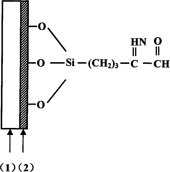
The invention relates to thin-film carrier material of tantalum-doped jewellers putty. The material comprises simple glass slide or monocrystalline silicon chip substrate material, thin films of tantalum-doped jewellers putty and an aldehyde group activity modificatory coat; and composition of the thin films of tantalum-doped jewellers putty has the following mass percent that Ta is between 0.8 percent and 8.2 percent; Sn is between 70.9 percent and 78 percent; and O is between 20.9 percent and 21.2 percent. The provided carrier material has the characteristics that the surface is flat and compact; the thickness is symmetrical; the active group has high density; the hydrophilicity is good; the chemical durability is high; the specific resistance is low and the organism compatibility is good, etc. The no marks electrics detecting, discrimination and analysis with high-sensitivity, high reliability and strong specificity can be realized on a biological signal. The carrier material adapts to a gene chip adopting the no marks electrics detecting technology. The thin-film carrier material of tantalum-doped jewellers putty also has the advantages that the preparation technology is simple and easy, the cost is low, and the industrialization production is easy to be realized, etc.

Description

technical field [0001] The invention relates to a tantalum-doped tin oxide thin film carrier material for a gene chip, in particular to a tantalum-doped tin oxide thin film carrier material for a gene chip suitable for a label-free electrical detection technology. Background technique [0002] Biochip technology represented by gene chips, because it can detect cells, proteins, nucleic acids, and other biomolecules accurately, quickly, and with high throughput, is widely used in the rapid diagnosis and treatment of diseases, the screening of new drugs, and pharmacogenomics. , gene mutation detection, optimal breeding of crops, judicial identification, environmental testing and national defense and many other fields have been widely used. However, despite the rapid development of gene chip technology for more than ten years, it still cannot become a technology that can be generally used in clinical medicine and experimental research, and it faces many key problems that need to...

Claims


Application Information

Patent Timeline
Patent Type & Authority Applications(China)
IPC IPC(8): C12Q1/68G01N27/00C03C17/34
Inventor 周荣张玉勤蒋业华
Owner KUNMING UNIV OF SCI & TECH
Learn More