Photoelectrical semiconductor component with 3-familty Ni compound semiconductor buffer layer and its making method

An optoelectronic semiconductor and manufacturing method technology, which is applied to semiconductor devices, electrical components, circuits, etc., can solve the problems of high hardness of the accumulated stress buffer layer, deterioration of epitaxial structure quality, lattice mismatch, etc.

Inactive Publication Date: 2008-09-17
ZHANJING TECH SHENZHEN +1
View PDF4 Cites 15 Cited by
  • Summary
  • Abstract
  • Description
  • Claims
  • Application Information

AI Technical Summary

Problems solved by technology

[0009] The aforementioned conventional technologies all use aluminum-containing nitride as a buffer layer. Due to the high hardness of the buffer layer, the lattice mismatch between the substrate and the light-emitting epitaxial structure cannot be adjusted.
The accumulated stress between the substrate and the light-emitting epitaxial st

Method used


Image

  • Photoelectrical semiconductor component with 3-familty Ni compound semiconductor buffer layer and its making method
  • Photoelectrical semiconductor component with 3-familty Ni compound semiconductor buffer layer and its making method
  • Photoelectrical semiconductor component with 3-familty Ni compound semiconductor buffer layer and its making method

Examples


Embodiment Construction

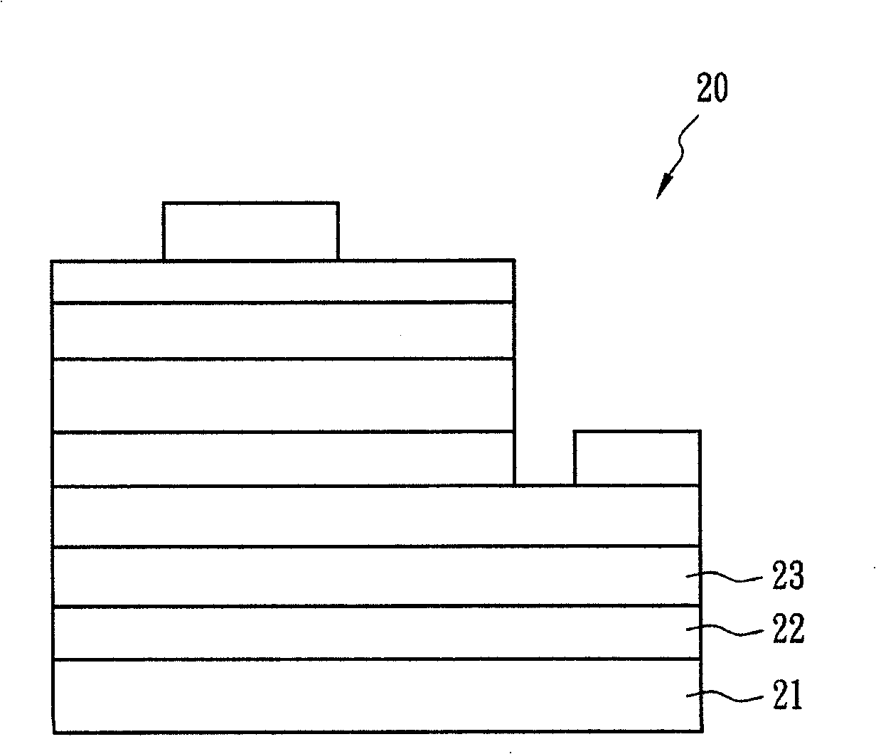
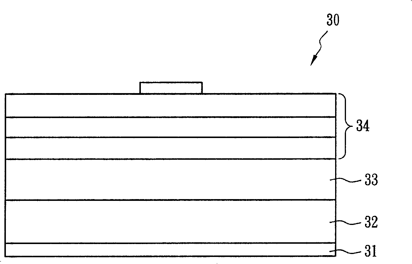
[0026] Figure 5 It is a structural diagram of the optoelectronic semiconductor component with P-type III nitrogen compound semiconductor of the present invention. Generally speaking, to make this optoelectronic semiconductor component 50 is to first provide a substrate 51, such as: sapphire (that is, aluminum oxide compound Al 2 o 3 ), silicon carbide (SiC), silicon, zinc oxide (ZnO), magnesium oxide (MgO), gallium arsenide (GaAs), etc., and different material layers are formed on the substrate 51 . Because the substrate 51 does not match the lattice constant of the III-group nitrogen compound, it is necessary to form at least two In on the substrate 51. x Ga 1-x N layer 521 and at least two In y Ga 1-yThe N layers 522 overlap a buffer layer 52 . Then grow an N-type semiconductor material layer 53 on the buffer layer 52 , which can be used as the N-type semiconductor material layer 53 to produce an N-type GaN-doped silicon thin film by epitaxy. Then grow an active laye...


PUM


Abstract

A photoelectric semiconductor component with three families nitrogen compound semiconductor buffer layers is provided, which comprises a substrate, and at least two InGa<1-x>N layers and at least two InGa<1-y>N layers which superimposes on the substrate alternately, wherein the x not equals to the y. A luminescent epitaxial structure is located on the surface of the InGa<1-y>N layer which is at the upper layer. A superlattice buffer layer is formed by the InGa<1-x>N layer which is between the substrate and the luminescent epitaxial structure and the InGa<1-y>N layer to reduce stress.

Description

technical field [0001] The invention relates to an optoelectronic semiconductor component with a buffer layer of a group III nitrogen compound semiconductor and its manufacturing method, in particular to an optoelectronic semiconductor component with a buffer layer of a group III nitrogen compound semiconductor. Background technique [0002] As light-emitting diode components are widely used in different products, materials for making blue light-emitting diodes have become an important research and development object for optoelectronic semiconductor materials in recent years. At present, the materials of blue light-emitting diodes include zinc selenide (ZnSe), silicon carbide (SiC) and indium gallium nitride (InGaN). above eV. Since the gallium nitride series is a light-emitting material with a direct gap, it can produce high-brightness illumination light, and has the advantage of longer life than zinc selenide, which also has a direct gap. [0003] The early research and ...

Claims


Application Information

Patent Timeline
IPC IPC(8): H01L33/00H01L33/02H01L33/12
Inventor 黄世晟涂博闵叶颖超徐智鹏詹世雄
Owner ZHANJING TECH SHENZHEN
Why Eureka
Try Eureka