Mach-zehnder type silicon optical waveguide switch based on narrow slit wave guide

A slit waveguide and waveguide switch technology, which is applied in the field of Mach-Zehnder type silicon optical waveguide switches, can solve the problems of limited application range, large absorption loss, and low extinction ratio, and achieve improved modulation efficiency, shortened pitch, and structural size compact effect

Inactive Publication Date: 2008-10-01
ZHEJIANG UNIV
View PDF0 Cites 22 Cited by
  • Summary
  • Abstract
  • Description
  • Claims
  • Application Information

AI Technical Summary

Problems solved by technology

However, the problem of slow thermo-optic modulation has not been solved, which seriously limits its application range.
Since the silicon material has no direct electro-optic effect, indirect electro-optic modulation can only be performed by carrier injection, which has large absorption loss, low extinction ratio, and the speed advantage cannot be well reflected.

Method used


Image

  • Mach-zehnder type silicon optical waveguide switch based on narrow slit wave guide
  • Mach-zehnder type silicon optical waveguide switch based on narrow slit wave guide
  • Mach-zehnder type silicon optical waveguide switch based on narrow slit wave guide

Examples


Embodiment 1

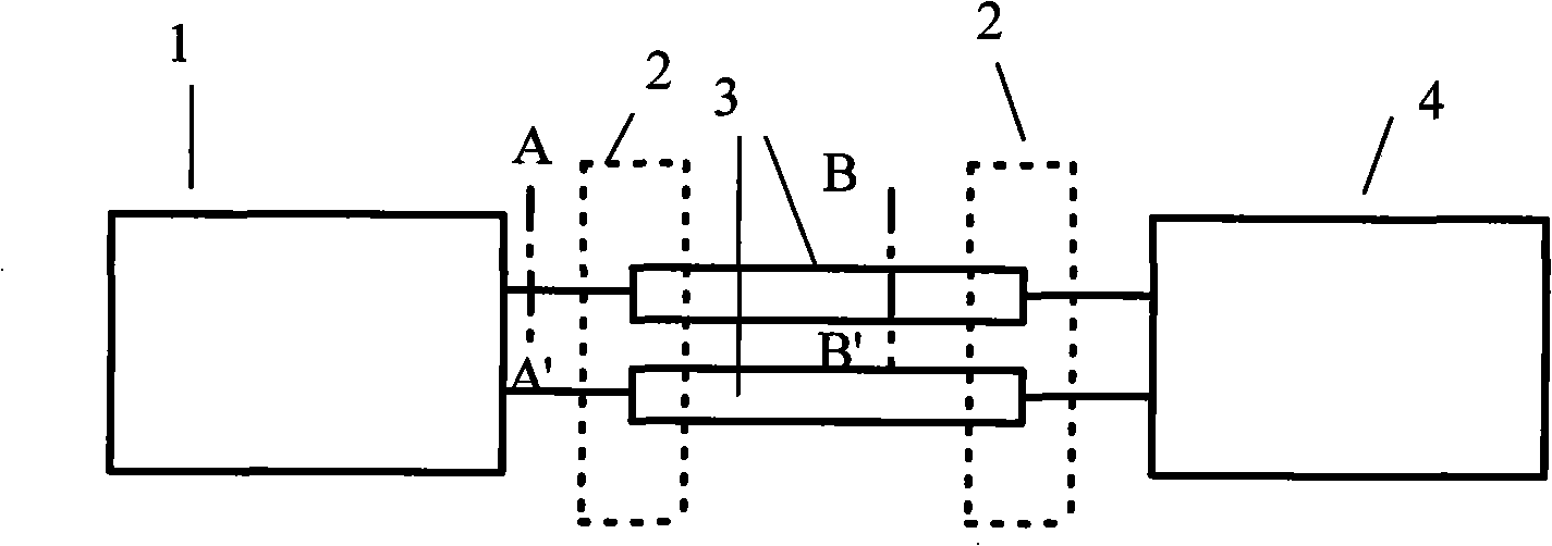
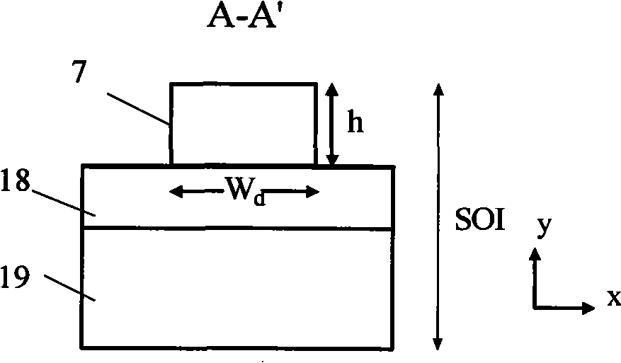
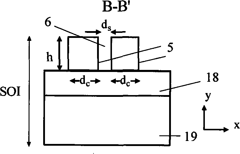
[0031] see Image 6 As shown, a 1×2 optical switch composed of a Y branch and an X structure is used. Take the SOI wafer with the top silicon thickness of 500 nanometers and the silicon dioxide buffer layer 18 thickness of 2 microns, thermally oxidize a layer of silicon dioxide on the top layer as a mask, and use the E-beam direct writing method to etch the device structure. . It includes a Y branch 10 for demultiplexing, a 9-mode spot conversion structure 2 for a tapered gradient waveguide pair composed of two silicon waveguides, an interference arm 3 for the slot waveguide structure, and an X junction 11 for combining waves. The electro-optical polymer DR1 / PMMA was covered by spin coating as the upper cladding layer and filled into the slits of the interference arms. The silicon waveguides 5 on both sides of the slit serve directly as electrodes.

[0032] When no phase modulation is applied, the guided wave is output from the wide-core waveguide 12; when one of the interf...

Embodiment 2

[0034] see Figure 7 shown, MMI-MZI type 1×2 optical switch. Take the SOI wafer with the top silicon thickness of 500 nanometers and the silicon dioxide buffer layer 18 thickness of 2 microns, thermally oxidize a layer of silicon dioxide on the top layer as a mask, and use the E-beam direct writing method to etch the device structure. . It includes a 1×2 MMI 16 for demultiplexing, an 8-mode spot conversion structure 2 consisting of a tapered gradient waveguide pair consisting of a single silicon waveguide, an interference arm 3 for a slot waveguide structure, and a 2×2 MMI 15 for combining waves. The device is immersed in liquid crystal, which acts as an upper cladding and fills the slits of the interference arms. The silicon waveguides 5 on both sides of the slit serve directly as electrodes.

[0035] When no modulation is applied, the light is output from the cross-state port. If modulation is applied to one of the phase-shift arms to produce a phase shift of π, the phas...

Embodiment 3

[0037] see Figure 8 As shown, the directional coupler constitutes a 2×2 optical switch. Take the SOI wafer with the top silicon thickness of 500 nanometers and the silicon dioxide buffer layer 18 thickness of 2 microns, thermally oxidize a layer of silicon dioxide on the top layer as a mask, and use the E-beam direct writing method to etch the device structure. . It includes a first directional coupler 17 that functions as a demultiplexer, a 9-mode spot conversion structure 2 composed of a tapered gradient waveguide pair composed of two silicon waveguides, an interference arm 3 of the slot waveguide structure, and a second wave-combining function. A directional coupler 11. The electro-optical polymer DR1 / PMMA was covered by spin coating as the upper cladding layer and filled into the slits of the interference arms. The silicon waveguides 5 on both sides of the slit serve directly as electrodes.

[0038] When unmodulated, the guided wave is output from the crossed state. ...


PUM


Abstract

The present invention discloses a Mach-Zehnder type silica optical waveguide switch based on narrow slit waveguide. After the wave splitting of the 3dB coupler which realizes power splitting function at the input end, a first group of two spot-size converting structures are respectively connected to the interference arms of two narrow slit waveguide structures, and then are connected to the output-end interference coupler through a second group of two spot-size converting structures. A random-structure 1*2 and 2*2 optical switches are formed through the different combination of two groups of spot-size converting structures. The present invention leads to a narrow slit waveguide and fills a low refraction ratio electrooptic material in the narrow slit. The modulation facility is enlarged, and the conventional indirect electrooptic modulation of carrier injection is switched to a direct electrooptic modulation. Besides, the silicon waveguides which are at two sides of the narrow slit and are electrically insulated naturally are taken as electrodes and the distance from the electrode to the modulation area is shortened. The two characteristics can equally increase the modulation efficiency of the switch. The whole structure is compact in dimension. The invention is compatible to the CMOS processing technique and provides a novel approach for the realization of the single-chip integrated high-speed electrooptic switch.

Description

technical field [0001] The invention relates to an optical communication device, in particular to a Mach-Zehnder type silicon optical waveguide switch based on a slit waveguide. Background technique [0002] Optical switch is one of the important components in optical communication and optical information processing system. The optical switches that have been realized so far include traditional mechanical structure optical switches, switches based on micro-optical electromechanical systems, liquid crystal optical switches, waveguide type optical switches, semiconductor optical amplifier optical switches and so on. Among them, the waveguide type optical switch developed by the integrated photonic technology has the advantages of low driving voltage, compact structure, large-scale array and can be integrated, and is an important development direction of the optical switch. [0003] As the pillar material of the rapidly developing microelectronics technology for more than 40 y...

Claims


Application Information

Patent Timeline
Patent Type & Authority Applications(China)
IPC IPC(8): G02F1/065G02B6/35H04B10/12
Inventor 肖司淼王翔王帆郝寅雷江晓清王明华杨建义
Owner ZHEJIANG UNIV
Why Eureka
Try Eureka