Method for preparing thin film type photon lattice structure GaN base LED

A technology of light-emitting diodes and photonic lattices, applied in semiconductor devices, electrical components, circuits, etc., can solve problems such as small tolerances, achieve the effect of reducing requirements and improving light extraction efficiency

Inactive Publication Date: 2008-10-08
江苏华功半导体有限公司
View PDF0 Cites 15 Cited by
  • Summary
  • Abstract
  • Description
  • Claims
  • Application Information

AI Technical Summary

Problems solved by technology

However, since the performance of the photonic lattice is very sensitive to changes in its structural parameters, the tolerance of structural control in the optical wavelength

Method used


Image

  • Method for preparing thin film type photon lattice structure GaN base LED
  • Method for preparing thin film type photon lattice structure GaN base LED
  • Method for preparing thin film type photon lattice structure GaN base LED

Examples


Embodiment Construction

[0030] Below in conjunction with accompanying drawing and specific embodiment the present invention is described in further detail:

[0031] 1. Preparation of GaN-based light-emitting diode (LED) chips

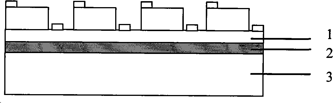
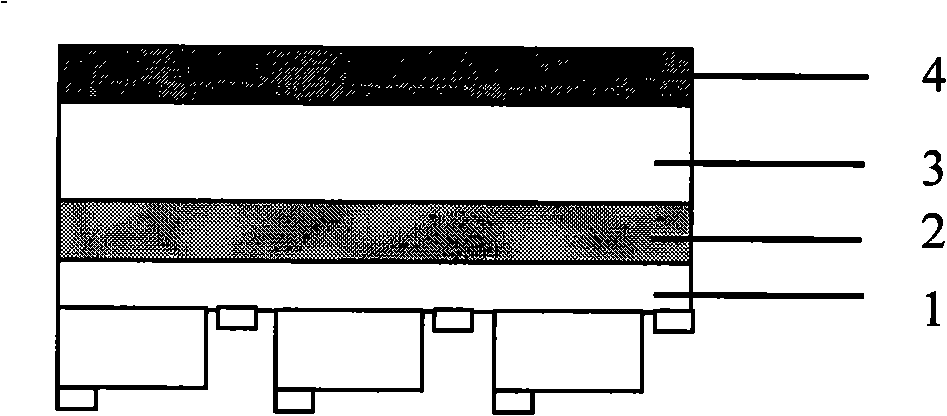
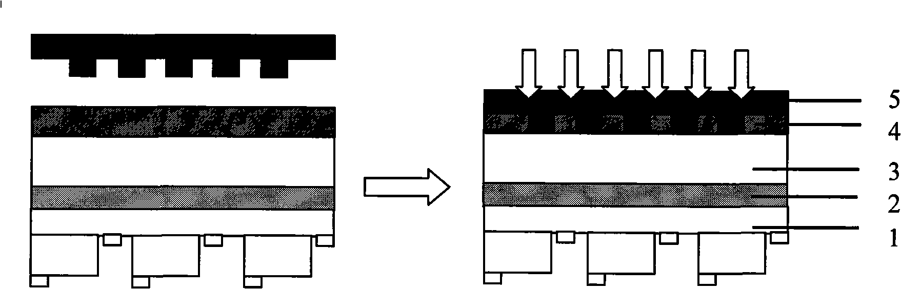
[0032] GaN-based LED materials including non-doped GaN layers are grown on sapphire substrates by epitaxial technology, such as figure 1 shown. That is, a layer of non-doped GaN is grown on the sapphire substrate with a thickness of 0.1-2 μm. Then grow an n-type GaN layer, multiple quantum wells, and a p-type GaN layer on the non-doped GaN layer, and prepare GaN-based light-emitting diodes (LEDs) by photolithography, dry etching, and metal deposition to form a sapphire substrate. on GaN-based chips.

[0033] Wherein, the stacking sequence of the n-type GaN layer, the multiple quantum wells and the p-type GaN layer determines whether the prepared light-emitting diode is a front-chip type or a flip-chip type.

[0034] The sapphire substrate can be polished or unpolished, wit...


PUM

PropertyMeasurementUnit
Thicknessaaaaaaaaaa
Energy densityaaaaaaaaaa
Thicknessaaaaaaaaaa

Abstract

The invention discloses a method for preparing a thin film type photon crystal lattice structure GaN-base luminescent diode, which belongs to field of GaN-base luminescent diode. The method includes: growing a multilayer GaN-base luminescent diode material on a sapphire substrate, which including a non-doping GaN layer, a n-type GaN layer, a multi-quantum trap and a p-type GaN layer; preparing a GaN-base luminescent diode on the GaN-base luminescent diode material; uniformly coating a layer of organic polymer on the sapphire substrate; forming a photon crystal lattice structure on the organic polymer by coining template; irradiating the sapphire substrate by laser from one surface of the organic polymer with the photon crystal lattice structure until the sapphire substrate and the non-doping GaN layer are separated, synchronously, forming a photon crystal lattice structure for the non-doping GaN layer. The method of present invention is adapted for preparing large-area thin film type photon crystal lattice structure GaN-base luminescent diode and can be industrially applied.

Description

technical field [0001] The invention relates to a preparation method of a GaN-based light-emitting diode (LED), in particular to a preparation method of a thin-film photonic lattice structure GaN-based light-emitting diode. Background technique [0002] The emergence and development of GaN-based LEDs has caused a revolution in solid-state lighting that has swept the world. Due to the limitation of internal total reflection, most of the light generated in LEDs is confined inside high-refractive index semiconductors. How to improve luminous efficiency is a challenge for the development of LEDs. The biggest challenge, theoretical research shows that the bottleneck to break through in the realization of semiconductor lighting is to improve luminous efficiency, which requires breakthroughs in science and technology. Since the GaN film is grown on a heterogeneous substrate such as sapphire, the poor quality of the material leads to limited space for improving the internal quantum ...

Claims


Application Information

Patent Timeline
IPC IPC(8): H01L33/00
Inventor 康香宁章蓓包魁代涛张国义
Owner 江苏华功半导体有限公司
Why Eureka
Try Eureka