Amorphous tungsten-doped tin dioxide transparent conductive oxide thin film and preparation method thereof

An oxide thin film, transparent and conductive technology, applied in semiconductor/solid-state device manufacturing, circuits, electrical components, etc., can solve the problems of low doping efficiency, etc., achieve high carrier mobility, stable performance, and high film deposition rate Effect

Inactive Publication Date: 2008-11-05
FUDAN UNIV
View PDF0 Cites 9 Cited by
  • Summary
  • Abstract
  • Description
  • Claims
  • Application Information

AI Technical Summary

Problems solved by technology

Usually, both of these situations will occur, and there will be recombi

Method used


Image

  • Amorphous tungsten-doped tin dioxide transparent conductive oxide thin film and preparation method thereof
  • Amorphous tungsten-doped tin dioxide transparent conductive oxide thin film and preparation method thereof
  • Amorphous tungsten-doped tin dioxide transparent conductive oxide thin film and preparation method thereof

Examples


Embodiment 1

[0019] Example 1, preparation of tungsten-doped tin dioxide ceramic target: grind and mix the mixed powder of chemically pure tin dioxide and tungsten evenly, sinter in air at 800°C for 12 hours, grind and mix evenly after cooling, and then grind and mix evenly at 13MPa Keep it under pressure for 10 minutes to form a target with a diameter of 25 mm and a thickness of 3 mm, and sinter at 850° C. for 12 hours to form a target. The substrate is an ordinary glass slide, which has been cleaned by pure water and alcohol ultrasonic waves for 15 minutes each.

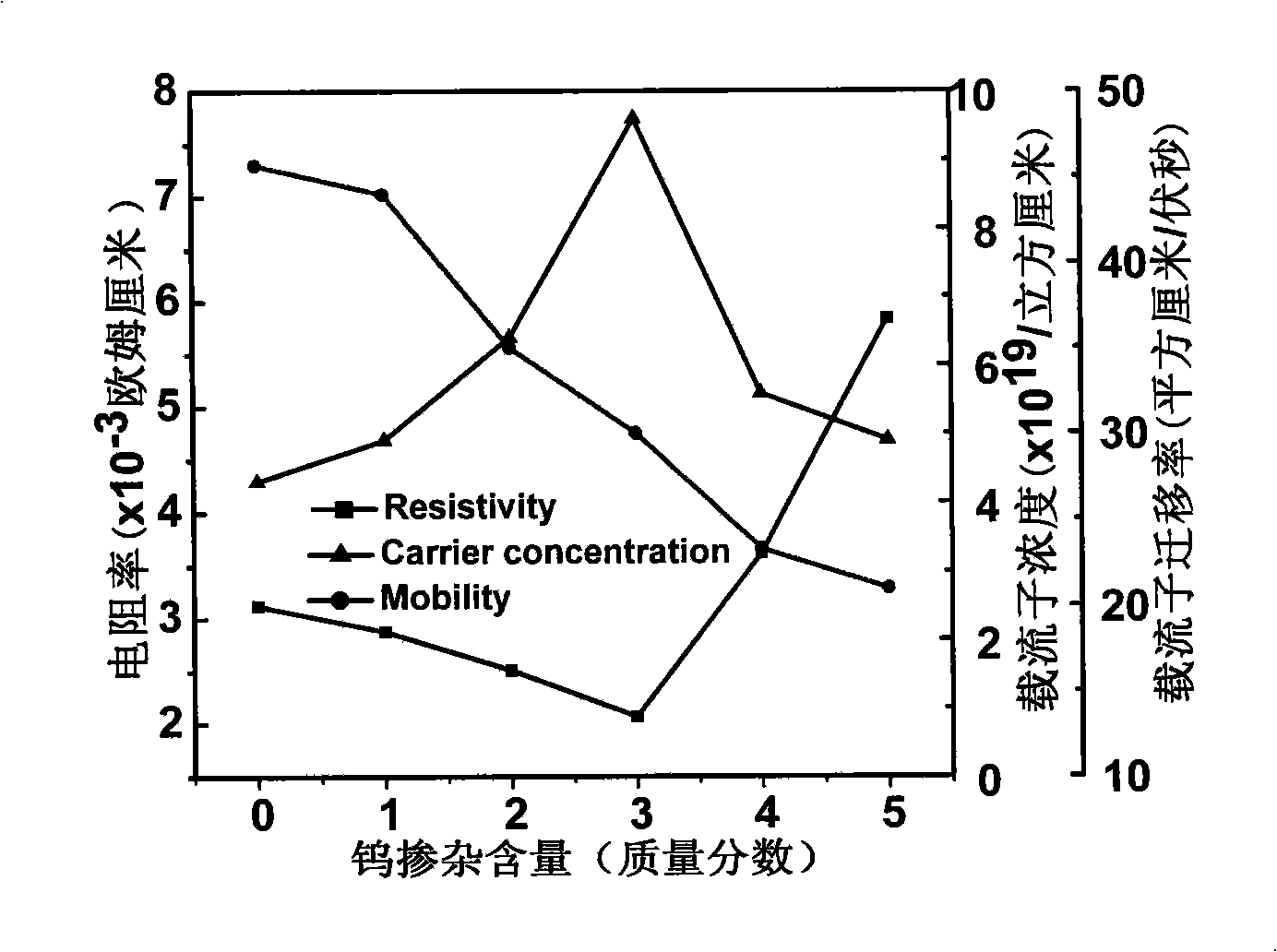
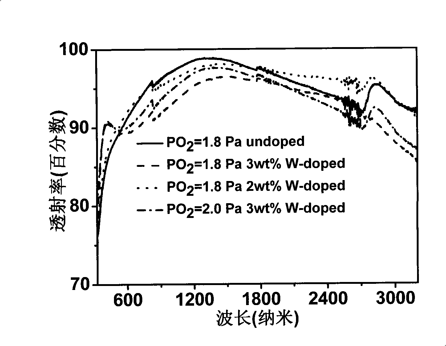
[0020] The tungsten doping content is 1 wt%. Before film deposition, the deposition chamber is evacuated to below 6.5×10 -3 Pa, then the O through the variable air pilot valve 2 and Ar gas into the vacuum chamber. The working pressure in the deposition chamber is 3.0Pa, the temperature of the ordinary glass substrate is 400°C, the oxygen partial pressure is 1.8Pa, the working current is 3.6mA, the working voltage is -16kV, a...

Embodiment 2

[0021] Example 2, preparation of tungsten-doped tin dioxide ceramic target: Grind and mix the mixed powder of chemically pure tin dioxide and tungsten evenly, sinter in air at 800°C for 12 hours, grind and mix evenly after cooling, and then grind and mix evenly at 13MPa Keep it under pressure for 10 minutes to form a target with a diameter of 25 mm and a thickness of 3 mm, and sinter at 850° C. for 12 hours to form a target. The substrates are ordinary glass slides and quartz glass, which are cleaned by pure water and alcohol ultrasonic waves for 15 minutes each.

[0022] The tungsten doping content is 3 wt%. Before film deposition, the deposition chamber is evacuated to below 6.5×10 -3 Pa, then the O through the variable air pilot valve 2 and Ar gas into the vacuum chamber. The working pressure in the deposition chamber is 3.0Pa, the ordinary glass substrate temperature is 400°C, the oxygen partial pressure is 1.2Pa, the working current is 3.6mA, the working voltage is -16...


PUM

PropertyMeasurementUnit
Thicknessaaaaaaaaaa
Thicknessaaaaaaaaaa
Carrier mobilityaaaaaaaaaa

Abstract

The invention belongs to the technical field of the transparent conductive film, particularly to the amorphous W-doped cassiterite transparent conductive film and the preparation method. The invention uses the cassiterite and the metal tungsten powder through the grinding, mixing, tabletting and sintering to obtain the block material as the target materials.Through the pulse plasma deposit (PPD) technology on the common glass substrate, SnO2:W film with the amorphous structure is prepared, wherein the film has the excellent optical and electrical performance of low resistivity, high carrier mobility, high visible light range transmissivity and high near infrared range transmissivity. The film obtained by the method can be applied with good application foreground in the flat panel display, the photoelectric sensor and the solar cell.

Description

technical field [0001] The invention belongs to the technical field of transparent conductive films, in particular to a tungsten-doped tin dioxide amorphous transparent conductive oxide film and a preparation method thereof. Background technique [0002] Transparent conductive oxide films (TCOs) have become indispensable materials in flat panel displays, solar cells, and transparent electronic devices due to their metal-like conductivity and transparency in the visible region. Tin-doped indium oxide (ITO) has always been the most commercially used transparent conductive material, but the reserves of metal indium are limited and cannot meet the growing market demand. In the past few years, its price has increased tenfold! Therefore, exploring alternative materials for ITO thin films has become one of the trends in the research of transparent conductive thin films in the future. At present, people are using various methods including process technology, selecting different mat...

Claims


Application Information

Patent Timeline
IPC IPC(8): H01L23/48H01L21/441H01L31/0224H01L31/18
CPCY02P70/50
Inventor 张群黄延伟李桂峰
Owner FUDAN UNIV
Why Eureka
Try Eureka