Nitrogen source ionization method and device for semiconductor material vapor deposition growth system

A vapor deposition, semiconductor technology, applied in the direction of polycrystalline material growth, crystal growth, chemical instruments and methods, etc., can solve the problems of high price, research field, production limitation, etc., and achieve the effect of good material growth quality

Inactive Publication Date: 2008-11-19
NANJING UNIV
View PDF0 Cites 6 Cited by
  • Summary
  • Abstract
  • Description
  • Claims
  • Application Information

AI Technical Summary

Problems solved by technology

At present, MOCVD systems for material growth are mostly imported from abroad in complete sets, and the price is expensive, and the research field and production are greatly restricted. The research and development of MOGVD systems with independent intellectual property rights has very important strategic significance [James J.Coleman, Metalorganic chemical vapor deposition for optoelectronic devices[C], Preceedings of the IEEE, 1997, 85(11)]

Method used


Image

  • Nitrogen source ionization method and device for semiconductor material vapor deposition growth system

Examples


specific Embodiment approach

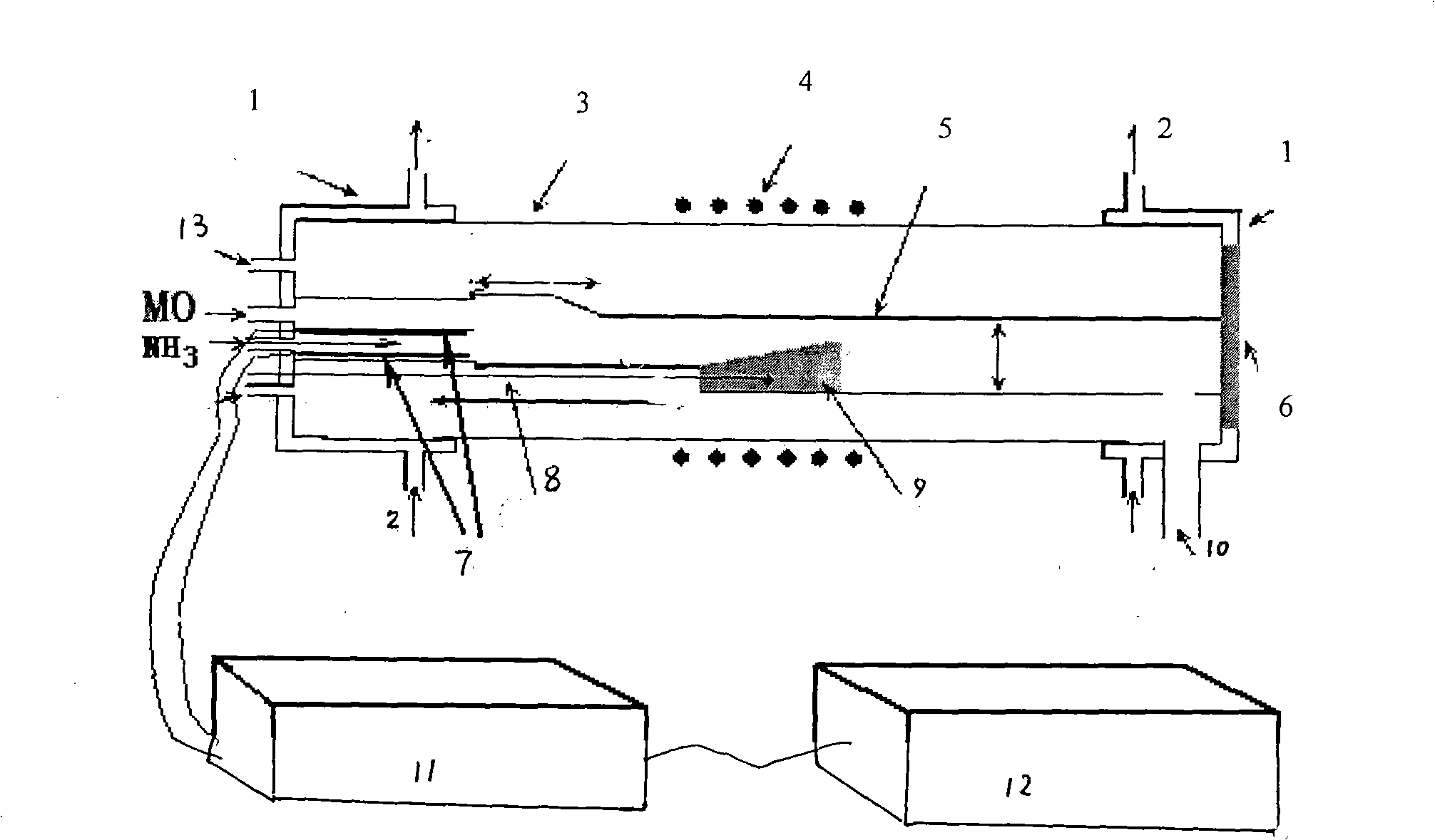
[0022] The invention relates to a novel nitrogen source ionization device used in semiconductor material growth systems such as CVD, MOCVD, HVPE and MBE. In order to improve the decomposition efficiency of ammonia molecules, parallel plate capacitors or cylindrical capacitors of radio frequency power are installed at the source inlets of nitride semiconductor growth equipment such as CVD and MOCVD. The ammonia gas is ionized by applying an external radio frequency field. The radio frequency discharge mode is a capacitive coupling type, that is, through a power matcher, a high frequency current is added to two parallel plate electrodes, and the electrons are accelerated by the electric field between the parallel capacitor plates to ionize. gas molecules, thereby creating a plasma in the parallel plates. The radio frequency capacitor can be used for ionization and decomposition of nitrogen sources that are not easy to be thermally decomposed at room temperature, such as the deco...


PUM


Abstract

The invention provides a nitrogen sources ionizing method applied to a gas phase deposition growth system of semiconductor materials. In a growth system of semiconductor materials such as CVD, MOCVD, HVPE and MBE, etc., an external radio frequency field is applied to ionize nitrogen sources. The high frequency electric current is applied to electrodes of capacitances or inductance coils, and the high frequency electric field is applied by a gas path arranged between the capacitance plates or circling the inductance coils to speed up electrons and ionize gas molecules to generate plasmas. The device consists of a metallic flange(1), a cooling water pipeline(2), a quartz outer cover(3), a quartz fairing(5), a metal cover(6), a parallel plate capacitor(7), a thermoelectric couple(8), graphite(9), a bleeder hole(10), a radio frequency adapter(11), a radio frequency power source(12) and an air inlet(13), wherein the metallic flange(1) and the metal cover(6) are arranged on both ends of the quartz outer cover(3), and the gas path circling the air inlet(13) or the gas path of a growth platform is provided with capacitances or inductance coupling elements.

Description

1. Technical field [0001] The invention relates to a novel nitrogen source ionization method and device for vapor deposition growth methods and systems, such as CVD, MOCVD, HVPE, MBE and other semiconductor material growth systems. 2. Background technology [0002] Group III-V compound semiconductor materials represented by GaN have extremely excellent optical, electrical, and thermodynamic properties: a wide band gap (314eV), can effectively emit light at a wavelength of 370nm, and can produce red to purple through doping Visible light; high electrical and thermal conductivity; high hardness (close to sapphire); high decomposition temperature (above 1000°C); good chemical stability (hardly corroded by any acid). [Zhang Rong, Yang Kai, Qin Linhong, etc., Research on the Properties of GaN Films Grown by MOCVD, Journal of Semiconductors, 1997, 18(2): 91; Zhang Qilin, Sun Wenhong, Liu Yanfei, etc., Research on the Growth of GaN Materials, Semiconductor Information, 1997, 34 (5...

Claims


Application Information

Patent Timeline
Patent Type & Authority Applications(China)
IPC IPC(8): C30B25/14C30B29/38
Inventor 谢自力张荣陶志阔崔旭高刘斌陈鹏修向前韩平赵红施毅郑有炓
Owner NANJING UNIV
Why Eureka
Try Eureka