Method for manufacturing semiconductor device and display device
A manufacturing method and display device technology, applied in semiconductor/solid-state device manufacturing, semiconductor devices, electric solid-state devices, etc., can solve problems such as complicated procedures, lower yield, and higher costs, so as to improve mass productivity and reduce crystallization process, the effect of increasing the film forming speed
- Summary
- Abstract
- Description
- Claims
- Application Information
AI Technical Summary
Problems solved by technology
Method used
Image

Examples
Embodiment approach 1
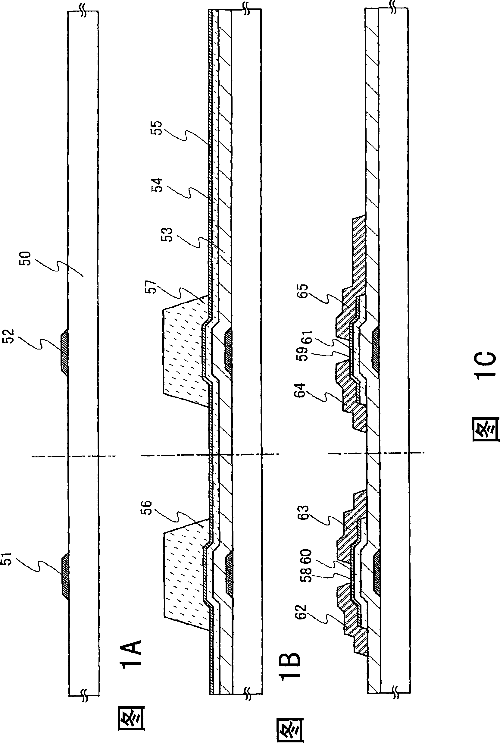
[0034] A method of manufacturing the display device of the present invention will be described. First, a description will be given using a light-emitting device as one embodiment of a display device. 1A to 1C , FIGS. 2A to 2C , and FIGS. 3A to 3C show a cross-sectional view of a thin film transistor used in a driver circuit, and a cross-sectional view of a thin film transistor used in a pixel portion. Note that an n-type thin film transistor using a microcrystalline semiconductor film has higher mobility than a p-type thin film transistor, and therefore an n-type thin film transistor is more suitable for use in a driver circuit. In the present invention, when thin film transistors having either polarity of n-type or p-type are used, it is preferable to make the polarities of the thin film transistors formed on the same substrate the same to reduce the number of steps.
[0035] As shown in FIG. 1A , a gate electrode 51 and a gate electrode 52 are formed on a substrate 50 . Th...
Embodiment approach 2
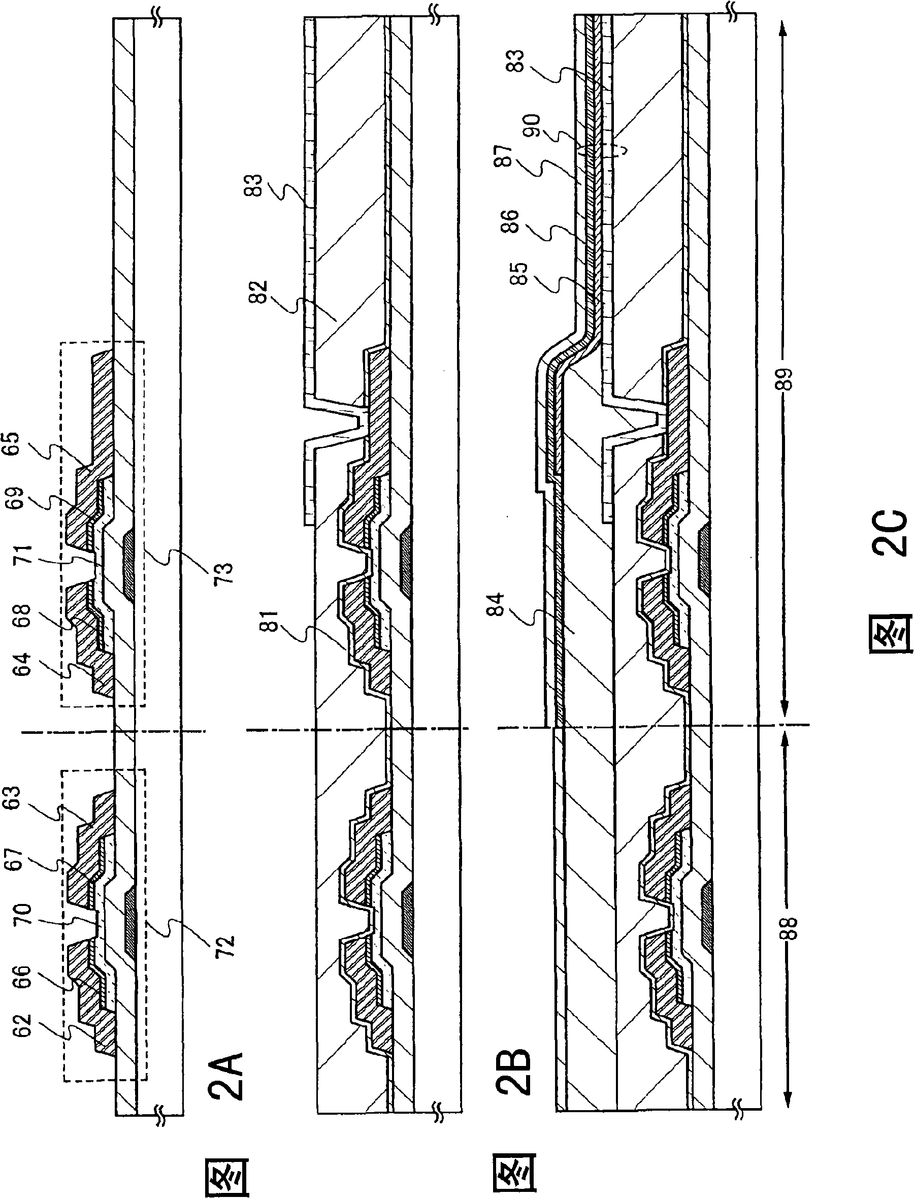
[0111] In this embodiment mode, other shapes of the thin film transistor shown in Embodiment Mode 1 will be described using FIG. 12 .
[0112] As shown in FIG. 12 , the TFTs 72 and 73 in this embodiment are characterized in that the ends of the source electrodes 62 a and 64 a do not coincide with the ends of the source regions 66 and 68 . In addition, it is also characterized in that the ends of the drain electrode 63 a and the drain electrode 65 a do not coincide with the ends of the drain region 67 and the drain region 69 .
[0113] In this embodiment mode, by using the same resist mask, the conductive film is wet-etched to form the source and drain electrodes 62a to 65a, and the semiconductor film to which an impurity element imparting one conductivity type is added is dry-etched to form the source region and the drain. Areas 66 to 69. By employing the structure of the source and drain electrodes 62a to 65a of this embodiment, since the distance between opposing electrodes...
Embodiment approach 3
[0115] Next, the structure of a display panel which is one embodiment of the display device of the present invention is shown below.
[0116] exist Figure 9 2 shows a mode of a display panel in which only the signal line driver circuit 6013 is formed and connected to the pixel portion 6012 formed on the substrate 6011 . The pixel portion 6012 and the scanning line driver circuit 6014 are formed using a thin film transistor using a microcrystalline semiconductor film. By forming a signal line driver circuit whose mobility is higher than that of a thin film transistor using a microcrystalline semiconductor film, the operation of the signal line driver circuit whose driving frequency is required to be higher than that required for scanning can be stabilized. The driving frequency of the line driver circuit. Note that the signal line driver circuit 6013 may be a thin film transistor using a single crystal semiconductor, a thin film transistor using a polycrystalline semiconduct...
PUM
 Abstract
Description
Claims
Application Information
 - Generate Ideas
- Intellectual Property
- Life Sciences
- Materials
- Tech Scout
- Unparalleled Data Quality
- Higher Quality Content
- 60% Fewer Hallucinations
Browse by: Latest US Patents, China's latest patents, Technical Efficacy Thesaurus, Application Domain, Technology Topic, Popular Technical Reports.
© 2025 PatSnap. All rights reserved.Legal|Privacy policy|Modern Slavery Act Transparency Statement|Sitemap|About US| Contact US: help@patsnap.com