Integrated circuit setting and production method especially for structuration

A technology of integrated circuits and production methods, applied in the field of setting and production of structured application-specific integrated circuits, can solve problems such as large static leakage and power consumption, and achieve the effects of high utilization rate and large flexibility

Inactive Publication Date: 2008-12-10
SHENZHEN STATE MICROELECTRONICS CO LTD
View PDF0 Cites 18 Cited by
  • Summary
  • Abstract
  • Description
  • Claims
  • Application Information

AI Technical Summary

Problems solved by technology

Many transistors in an FPGA are used for buffering, look-up tables, and switching, not just logic, and the static leakage power is quite large

Method used


Image

  • Integrated circuit setting and production method especially for structuration
  • Integrated circuit setting and production method especially for structuration
  • Integrated circuit setting and production method especially for structuration

Examples


Embodiment Construction

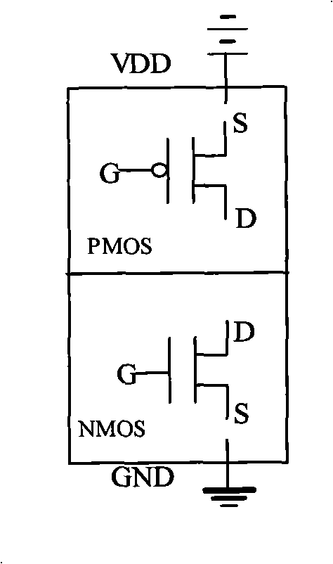
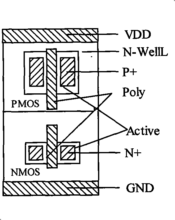
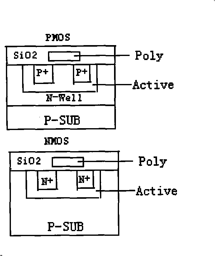
[0029] The present invention will be further described in detail below with reference to the drawings and embodiments. Such as Picture 1-1 , Figure 1-2 with Figure 1-3 As shown, in the method of the present invention, the small-granularity macro cell GCELL is set up to establish an N-channel metal-oxide-semiconductor field effect transistor NMOS on a P-type silicon substrate P-sub, and N-well in the N-well region The P-channel metal-oxide-semiconductor field effect transistor PMOS is established inside. The drain terminal D, source terminal S, and gate G of the NMOS tube and PMOS tube are all suspended, and the length and width of the CELL are grids (the minimum wiring pitch is the unit Grid). In the circuit structure, the PMOS tube and NMOS tube are connected to other circuit parts of the outside world through the drain D, source S, and gate G to realize a complete circuit; in terms of the physical structure, the polysilicon poly, high-concentration P-type ion doped area P + Z...


PUM


Abstract

The invention discloses arrangement of a structured special integrated circuit, and a manufacturing method thereof, to solve the technical problem of saving development cost and reducing development period. The method of the invention comprises the following steps of: 1, undergoing arrangement and manufacturing on a master slice, for arranging a universal function module and a cell library of a special integrated circuit, and producing universal level for the master slice; 2, arranging and producing the special chip, for arrangement of the special integrated circuit and production of residual level based on the master slice. Compared with current technology, the invention takes full advantage of current tool based on establishment of the cell library, and implements structured ASIC technology, with great flexibility and high utility ratio of small-grained macro cell. Any product implemented by the structured technology has a digital function part decomposed into macro cell array physically. A new product can be implemented conveniently and fast on the master slice through generation of ohm contact, a through hole and a metal layer.

Description

Technical field [0001] The invention relates to an integrated circuit setting and production method, in particular to a structured application specific integrated circuit setting and production method. Background technique [0002] After the integrated circuit technology has entered deep sub-micron, the problems of cost and reliability have become the bottleneck for the development of ASIC (Application Specific Integrated Circuit). For example, standard cell ASIC wiring at the 90nm node is both expensive and risky. As the settings tend to adopt smaller process sizes, the non-repetitive investment in NRE, including the mask composition cost, and the investment in engineering settings such as layout and verification, are increasing. Therefore, it is very important to realize the correct device function the first time. Field Programmable Gate Array FPGA (FieldProgrammable Gate Array) has the characteristics of real-time reprogramming and online verification, which has made it develo...

Claims


Application Information

Patent Timeline
Patent Type & Authority Applications(China)
IPC IPC(8): H01L21/82G06F17/50
Inventor 祝昌华谢文刚刘建新张满仓贾柱良
Owner SHENZHEN STATE MICROELECTRONICS CO LTD
Why Eureka
Try Eureka