Semiconductor apparatus and method for fabricating the same
A manufacturing method and semiconductor technology, applied in semiconductor/solid-state device manufacturing, semiconductor devices, electric solid-state devices, etc., can solve the problems of increased risk of dimensional changes, easy concentration of electric field, etc.
- Summary
- Abstract
- Description
- Claims
- Application Information
AI Technical Summary
Problems solved by technology
Method used
Image

Examples
Embodiment 1、2
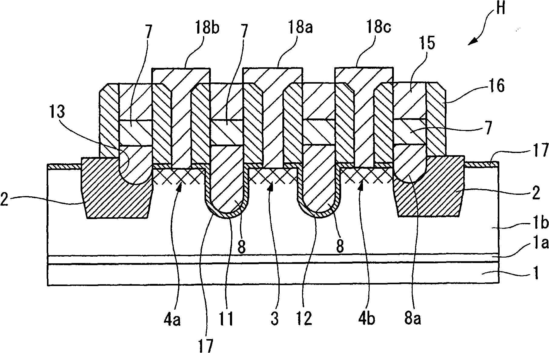
[0149] Optimum conditions for the photosensitive hydrogen bake and photosensitive DCE oxidation of the present invention were investigated for samples using hydrogen bake and oxidation method optimum conditions, producing Si flashes after silicon dry etching of trenches.
[0150] (sample construction)
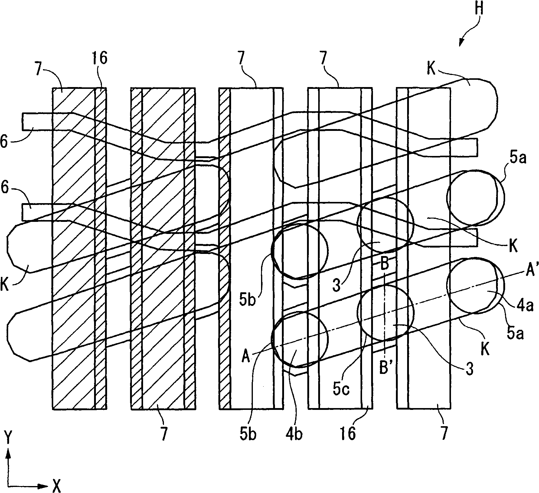
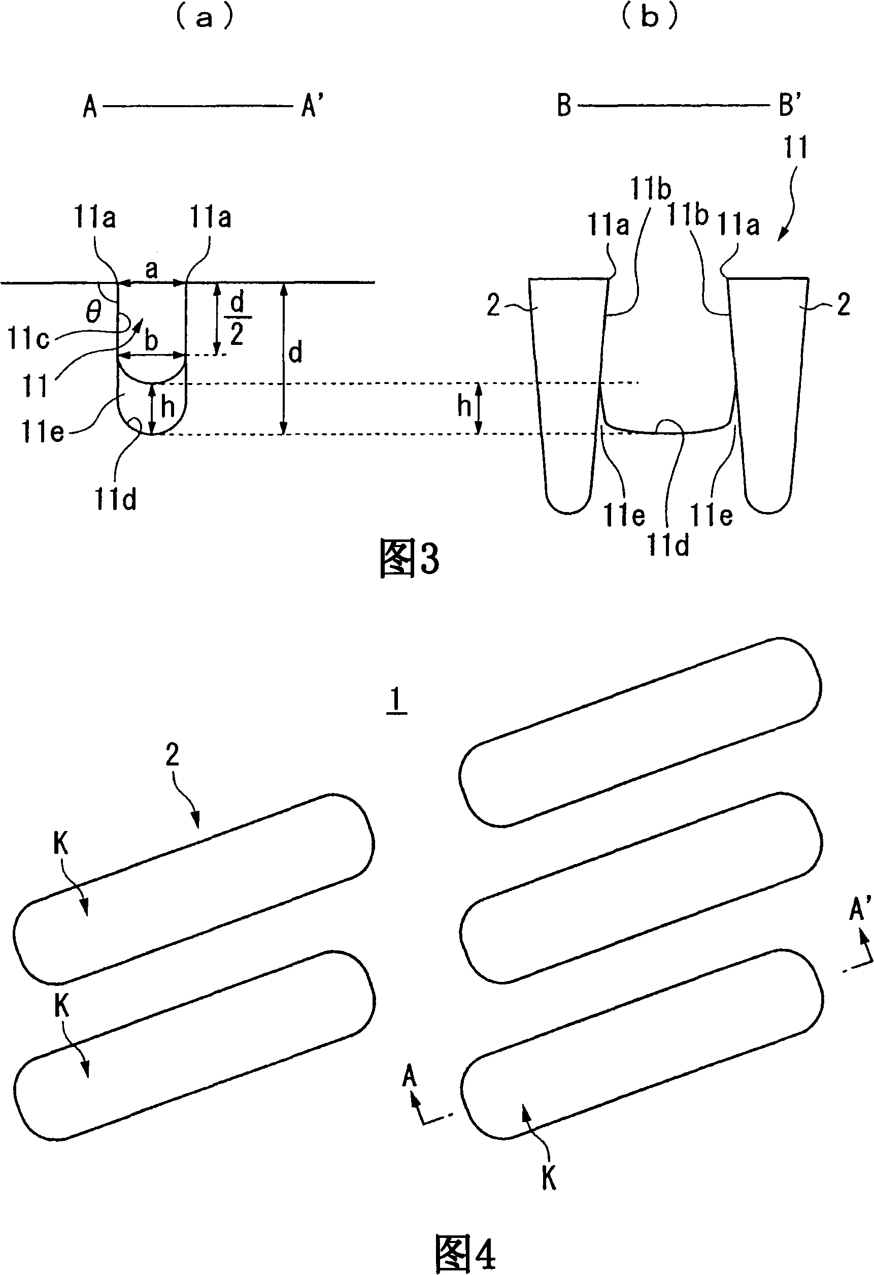
[0151] The shape after dry etching is as follows Figure 5 the shape shown.
[0152] (Dry Etching Device)
[0153] A commercially available ICP plasma etching apparatus was used.
[0154] (Silicon dry etching conditions)
[0155] HBr / Cl 2 / O 2 =100 / 90 / 10sccm, 10mTorr (1.33Pa), RF (upper / lower)=500W / 100W (Stage temperature=10°C).
[0156] (Hydrogen baking reference conditions)
[0157] h 2 =15 L / min, 20Torr (2.67×10 3 Pa), 850°C, 600 sec.
[0158] The conditions required for hydrogen baking must meet the following two conditions at the same time:
[0159] (1) The height of Si flash is as low as about 20% of the initial height;
[0160] (2) The oxide film on the trenc...
Embodiment 3
[0178] Next, the optimum temperature and time conditions for the most effective DCE oxidation were investigated. Optimum time (50, 100, 150, 200 seconds) was studied in order to keep the temperature at 850° C., which is the lower limit set in the equipment used, so that the oxide film does not apply to the Si flash portion. The upper film thickness a', middle film thickness b', and bottom film thickness c' were measured, and their ratios (a' / b', b' / c') were calculated. The results are shown in Table 3.
[0179] table 3
[0180] Example 3
Comparative Example 8
Comparative Example 9
Comparative Example 10
Oxidation treatment time
(Second)
100
50
150
200
upper film thickness
(a')
1.5
1.0
1.8
2.1
Intermediate film thickness
(b')
1.3
0.85
15
1.8
Bottom Film Thic...
Embodiment 4
[0194] As a comparison with other processing methods, several methods were tried to remove the Si flash on the STI side generated in the dry etching process when trench gates are formed in DRAM, and their shapes were compared.
[0195] (sample construction)
[0196] The shape after dry etching is as follows Figure 5 the shape shown.
[0197] (Dry Etching Device)
[0198] A commercially available ICP plasma etching apparatus was used.
[0199] (Silicon dry etching conditions)
[0200] HBr / Cl 2 / O 2 =100 / 90 / 10sccm, 10mTorr (1.33Pa), RF (upper / lower)=500W / 100W (Stage temperature=10°C).
[0201] (Chemical Dry Etching Conditions)
[0202] CF 4 / Ar=100 / 100sccm, Pressure=20mTorr (2.67Pa), RF (upper / lower)=500W / 0W (Stage temperature=10°C).
[0203] (hydrogen bake only)
[0204] Hydrogen baking condition: H 2 =15 L / min, 20Torr (2.67×10 3 Pa), 875°C, 60sec.
[0205] (Method of the present invention: hydrogen baking+DCE oxidation)
[0206] Photosensitive hydrogen baking co...
PUM
 Abstract
Description
Claims
Application Information
 - Generate Ideas
- Intellectual Property
- Life Sciences
- Materials
- Tech Scout
- Unparalleled Data Quality
- Higher Quality Content
- 60% Fewer Hallucinations
Browse by: Latest US Patents, China's latest patents, Technical Efficacy Thesaurus, Application Domain, Technology Topic, Popular Technical Reports.
© 2025 PatSnap. All rights reserved.Legal|Privacy policy|Modern Slavery Act Transparency Statement|Sitemap|About US| Contact US: help@patsnap.com