Method for MOVCD growth nitride epitaxial layer

A technology of nitride epitaxial layer and growth temperature, which is applied in coating, gaseous chemical plating, metal material coating process, etc., can solve the problems of reducing the quality of epitaxial wafers, easily forming damaged layers and pollution on the surface of sapphire substrates

Inactive Publication Date: 2009-01-14
EPILIGHT TECH +2
View PDF1 Cites 18 Cited by
  • Summary
  • Abstract
  • Description
  • Claims
  • Application Information

AI Technical Summary

Problems solved by technology

[0004] However, during the growth process of this process, a damaged layer and contamination are easily formed on the surface of the sapphire substrate, thereby reducing the quality of the epitaxial wafer.

Method used


Image

  • Method for MOVCD growth nitride epitaxial layer
  • Method for MOVCD growth nitride epitaxial layer

Examples


Embodiment Construction

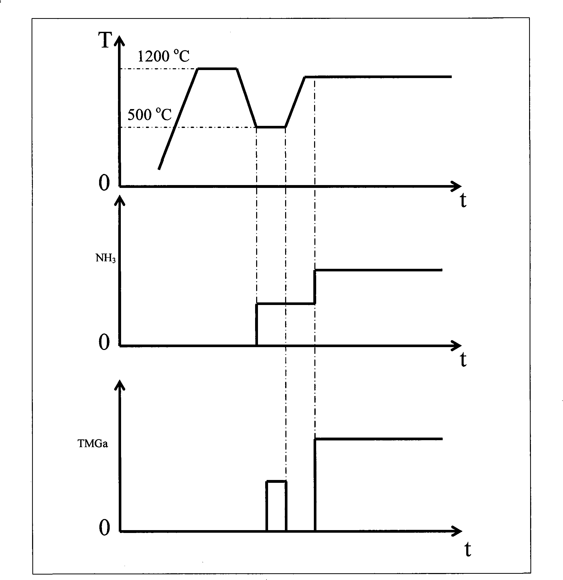
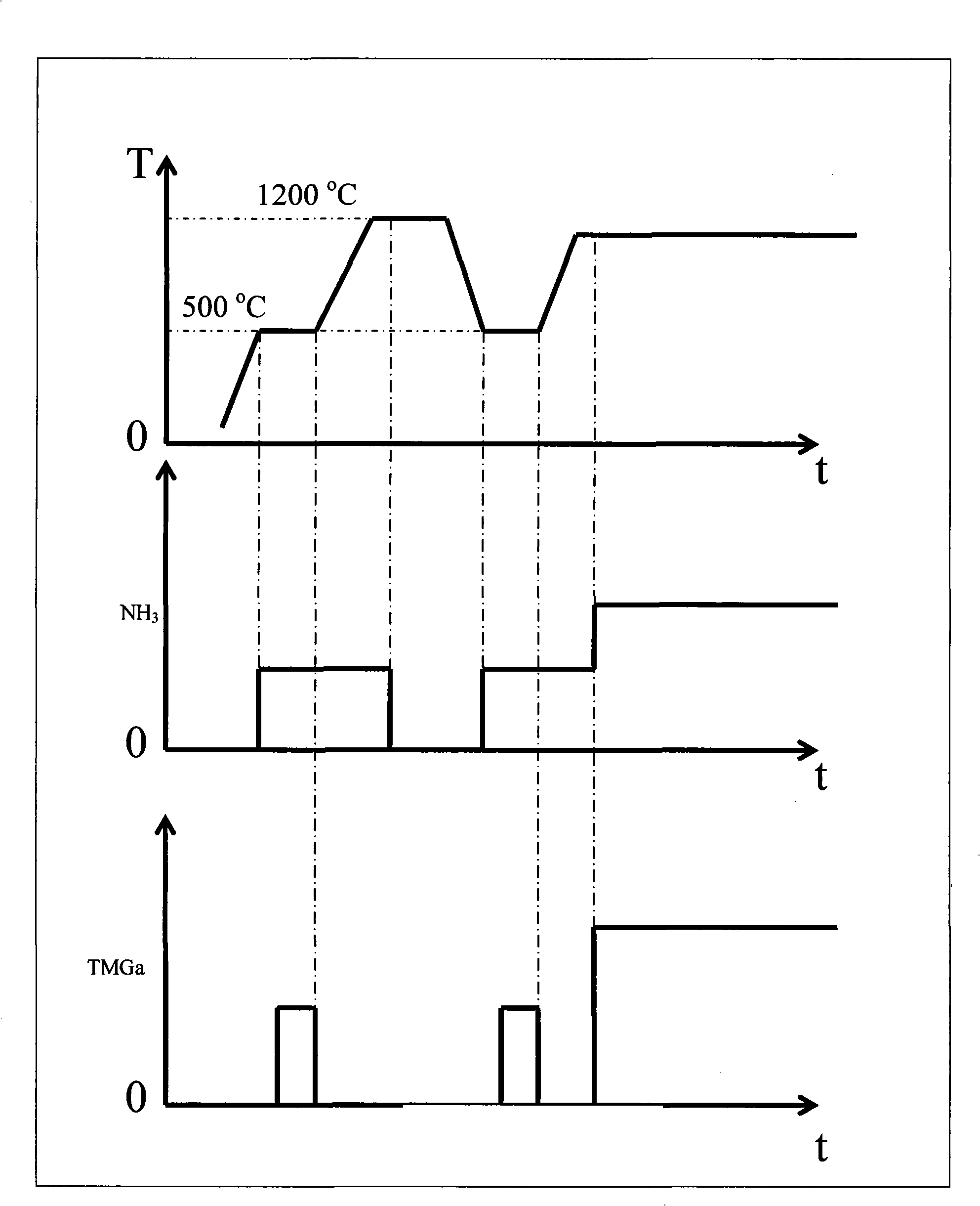
[0030] Further illustrate the specific implementation steps of the present invention below in conjunction with accompanying drawing:

[0031] A method for growing a nitride epitaxial layer with MOVCD, which adopts MOCVD technology, uses high-purity NH3 as N source, high-purity H2 or N2 as carrier gas, trimethylgallium (TMGa) or triethylgallium (TEGa) and three Indium methyl (TMIn) and trimethylaluminum (TMAl) do Ga source and In source and Al source respectively; Substrate is sapphire (Al2O3); The method comprises the following steps:

[0032] Step 1, in the MOCVD reaction chamber, the sapphire substrate is heated to a relatively low temperature, preferably between 500°C and 900°C, with H2 or N2 gas as the carrier gas, and trimethylgallium (TMGa) and NH3 grows a GaN layer on the surface of sapphire; its thickness is preferably controlled between 10 nm and 200 nm. This layer of GaN is called the sacrificial layer;

[0033]Step 2, after the growth of the GaN sacrificial layer ...


PUM

PropertyMeasurementUnit
thicknessaaaaaaaaaa

Abstract

The invention relates to a method to generate nitride epitaxial layer and nitride light emitting diode structure epitaxial wafer through MOVCD. The MOVCD technology is adopted, high purity NH3 is utilized as N source, high purity H2 or N2 is utilized as the carrier gas, and trimethyl gallium (TMGa) or triethyl gallium (TEGa), trimethyl indium (TMIn) and trimethyl aluminium (TMAl) are respectively utilized as Ga source, In source and Al source; the substrate adopts sapphire (Al2O3); the sapphire substrate is heated to 500 DEG C in the MOCVD reaction chamber, in the atmosphere of H2, trimethyl gallium (TMGa) is filled to generate a GaN layer, in the high temperature (1200 DEG C) H2 atmosphere, reaction is generated between GaN and the sapphire(Al2O3) on the substrate surface, the surface damage and the surface pollution of the sapphire can be better removed, micro pits of the nanometer grade can be corroded on the sapphire surface, the micro pits is favorable to the improvement of the epitaxial layer, and to the most important, the LED emitting efficiency is enhanced.

Description

technical field [0001] The invention relates to a metal organic vapor deposition (MOCVD) epitaxial growth method of a III-V nitride material based on gallium nitride (GaN), in particular to a growth method of a nitride multi-quantum light-emitting diode structure epitaxial wafer. Background technique [0002] The new generation of semiconductor materials represented by GaN has attracted widespread attention due to its wide direct bandgap (Eg=3.4eV), high thermal conductivity, high hardness, high chemical stability, low dielectric constant, and radiation resistance. It has great application potential in the fields of solid-state lighting, solid-state lasers, optical information storage, and ultraviolet detectors. Calculated according to China's electricity consumption in 2002, if solid-state lighting is used to replace traditional light sources, the power generation of the Three Gorges Hydropower Station can be saved a year, which will have huge economic, environmental and so...

Claims


Application Information

Patent Timeline
Patent Type & Authority Applications(China)
IPC IPC(8): C23C16/34C23C16/455C23C16/52
Inventor 郝茂盛潘尧波颜建锋周建华孙永健杨卫桥陈志忠张国义
Owner EPILIGHT TECH
Why Eureka
Try Eureka