Method and chip for integrating micro electromechanical system device and integrated circuit

A technology of micro-electromechanical systems and integrated circuits, applied in the direction of electric solid-state devices, chemical instruments and methods, piezoelectric/electrostrictive/magnetostrictive devices, etc., can solve the problems of high packaging cost, overall performance degradation, and multiple interference Signal and other issues, to achieve the effect of reducing packaging cost, reducing volume, and reducing packaging cost

Active Publication Date: 2009-01-28
MEMSENSING MICROSYST SUZHOU CHINA
View PDF0 Cites 19 Cited by
  • Summary
  • Abstract
  • Description
  • Claims
  • Application Information

AI Technical Summary

Problems solved by technology

The scheme firstly manufactures MEMS devices and integrated circuits separately on different chips, then mounts them adjacently on the same substrate, and electrically connects them through wire bonding, and then conducts ceramic or metal packaging to Complete integration, the disadvantage of this scheme is that the electrical connection between the two is realized by a long lead wire, which will introduce more interference signals, which

Method used


Image

  • Method and chip for integrating micro electromechanical system device and integrated circuit
  • Method and chip for integrating micro electromechanical system device and integrated circuit
  • Method and chip for integrating micro electromechanical system device and integrated circuit

Examples


Embodiment Construction

[0034] The method for integrating MEMS devices and integrated circuits and the formed integrated chips of the present invention will be described in detail below through specific embodiments.

[0035] see figure 1 and Figure 13 , the integration method of MEMS device and integrated circuit of the present invention mainly comprises the following steps:

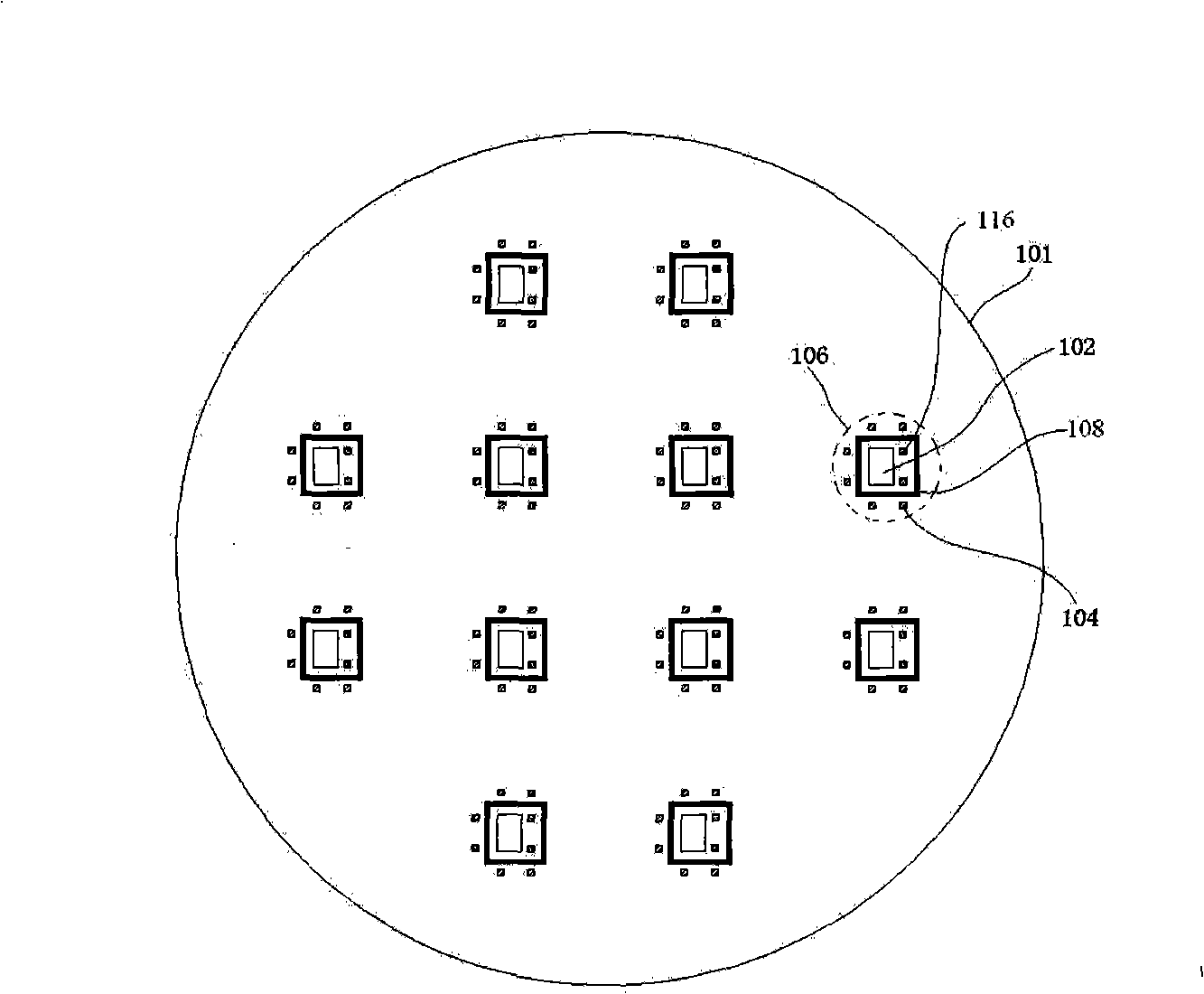
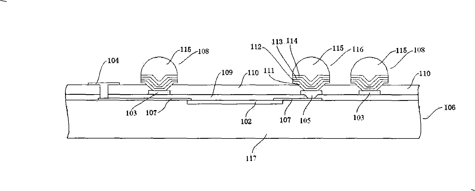
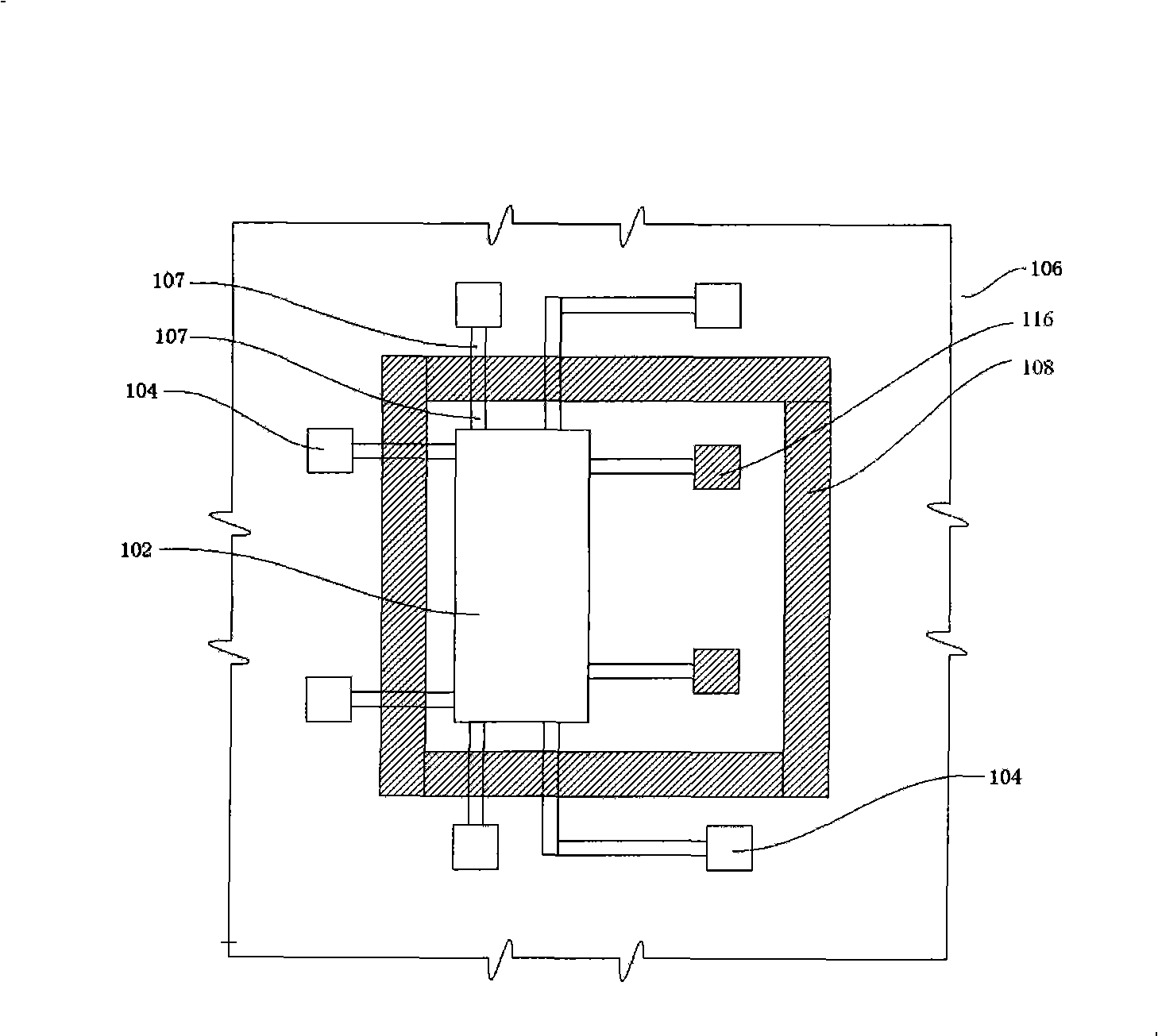
[0036] The first step: provide a first wafer 201 and a second wafer 101 respectively, such as Figures 4 to 6 As shown, the first wafer 201 has a plurality of first chips, that is, MEMS device units 205, each MEMS device unit 205 is composed of 3 layers, the bottom layer is a silicon substrate 208, and the silicon substrate There is a silicon oxide layer 216 on the silicon oxide layer 208, and a device layer 206 is on the silicon oxide layer 216. A narrow groove 219 is obtained by photolithography and etching to form a MEMS device such as a comb-tooth capacitance accelerometer 202. The accelerometer A release hole 215 is ge...


PUM


Abstract

The invention provides an integration method and an integrated chip for a micro-electronic-mechanical-system device and an integrated circuit. The method comprises the following steps of: firstly, providing a first chip provided with a first electric connection point and the MEMS device, and a second chip provided with a second electric connection point and the integrated circuit; then, generating a first additional conductive point on the first electric connection point, and simultaneously generating a first package ring surrounding the MEMS device; generating a second additional conductive point on the second electric connection point, and simultaneously generating a second package ring on the second chip; finally, leading the first chip and the second chip in abutting joint, leading the first additional conductive point and the second additional conductive point to be fused in abutting joint to complete the electric connection of the MEMS device and the integrated circuit, simultaneously, leading the first package ring and the second package ring to be fused in abutting joint to package the MEMS device in the ring, thereby reducing the package cost, simultaneously shortening the electric connection route between the MEMS device and the integrated circuit, and effectively reducing stray capacitance and coupling inductance.

Description

technical field [0001] The invention relates to an integration method and an integrated chip of a micro-electromechanical system (MEMS) device and an integrated circuit. Background technique [0002] MEMS technology is a high-tech development in recent years. Compared with corresponding devices made by traditional technology, devices made by MEMS technology have obvious advantages in volume, power consumption, weight and price, and it adopts advanced semiconductor manufacturing technology, which can realize batch manufacturing of MEMS devices. In the market, the main application examples of MEMS devices include pressure sensors, accelerometers and silicon microphones. [0003] MEMS devices need to be connected and integrated with integrated circuits (CMOS / Bipolar) such as drive, detection, and signal processing to become a system with complete independent functions. At present, there are many kinds of integration schemes. The production of circuits and MEMS devices on the ...

Claims


Application Information

Patent Timeline
IPC IPC(8): H01L21/50H01L21/56H01L21/60H01L25/00H01L23/31H01L23/488B81C5/00B81C99/00
CPCH01L24/11H01L2224/11H01L2924/14H01L2924/1461H01L2924/00H01L2924/00012
Inventor 李刚胡维
Owner MEMSENSING MICROSYST SUZHOU CHINA
Why Eureka
Try Eureka