Method for preparing vertical structure LED using whole optical film system

A light-emitting diode, vertical structure technology, applied in semiconductor devices, electrical components, circuits, etc., can solve the problems of low light extraction efficiency, poor heat dissipation capacity, uneven current distribution, etc.

Active Publication Date: 2009-01-28
INST OF SEMICONDUCTORS - CHINESE ACAD OF SCI
View PDF0 Cites 25 Cited by
  • Summary
  • Abstract
  • Description
  • Claims
  • Application Information

AI Technical Summary

Problems solved by technology

However, the current luminous efficiency of white LEDs is still far from the 160-200lm / w required by general lighting. Uneven current distribution, low light extraction efficiency and poor heat dissipation are the main problems facing the development of power LEDs. technical bottleneck
The vertical structure LED is a new solution based on the above problems. Compared with the traditional front-mounted structure and flip-chip structure LEDs, the vertical structure of the upper and lower electrodes can effectively solve the problems of uneven current distribution and poor heat dissipation. Optical properties, i.e. no significant improvement in extraction efficiency

Method used


Image

  • Method for preparing vertical structure LED using whole optical film system
  • Method for preparing vertical structure LED using whole optical film system
  • Method for preparing vertical structure LED using whole optical film system

Examples


Embodiment Construction

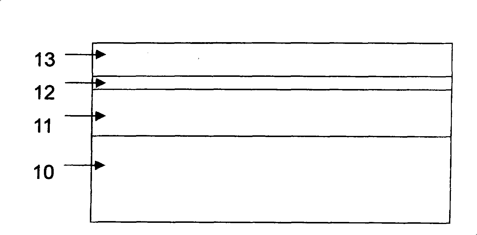
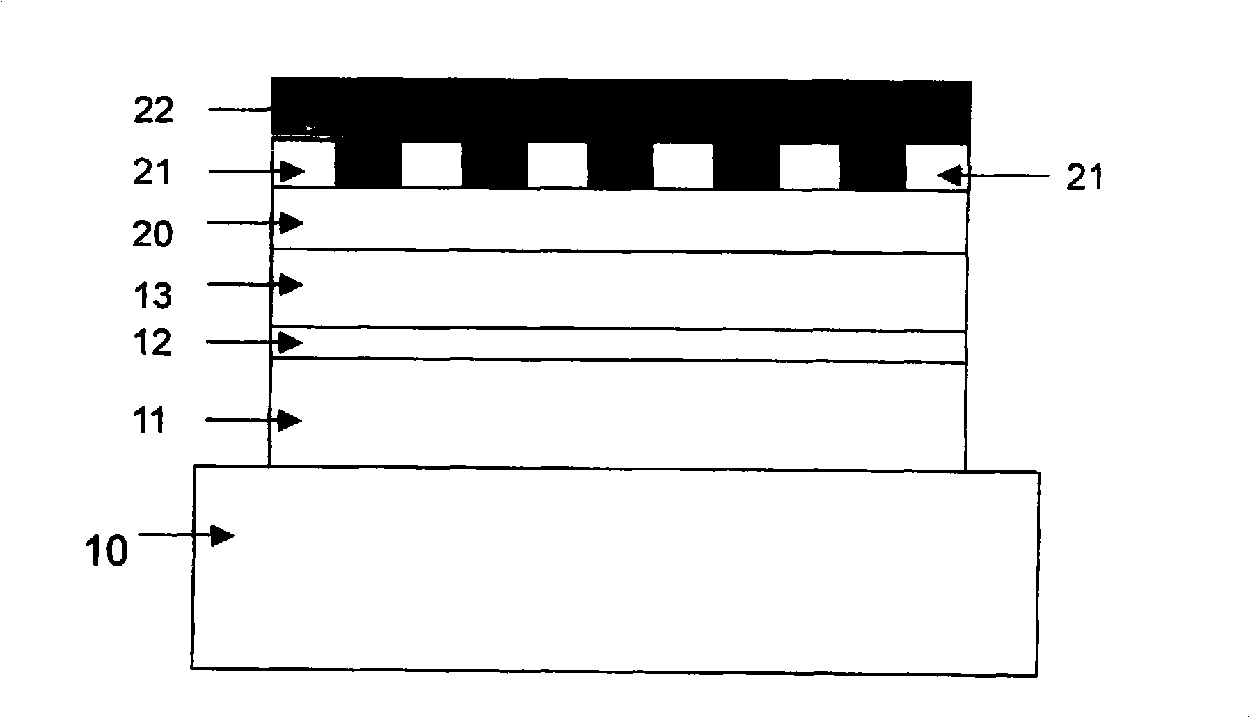
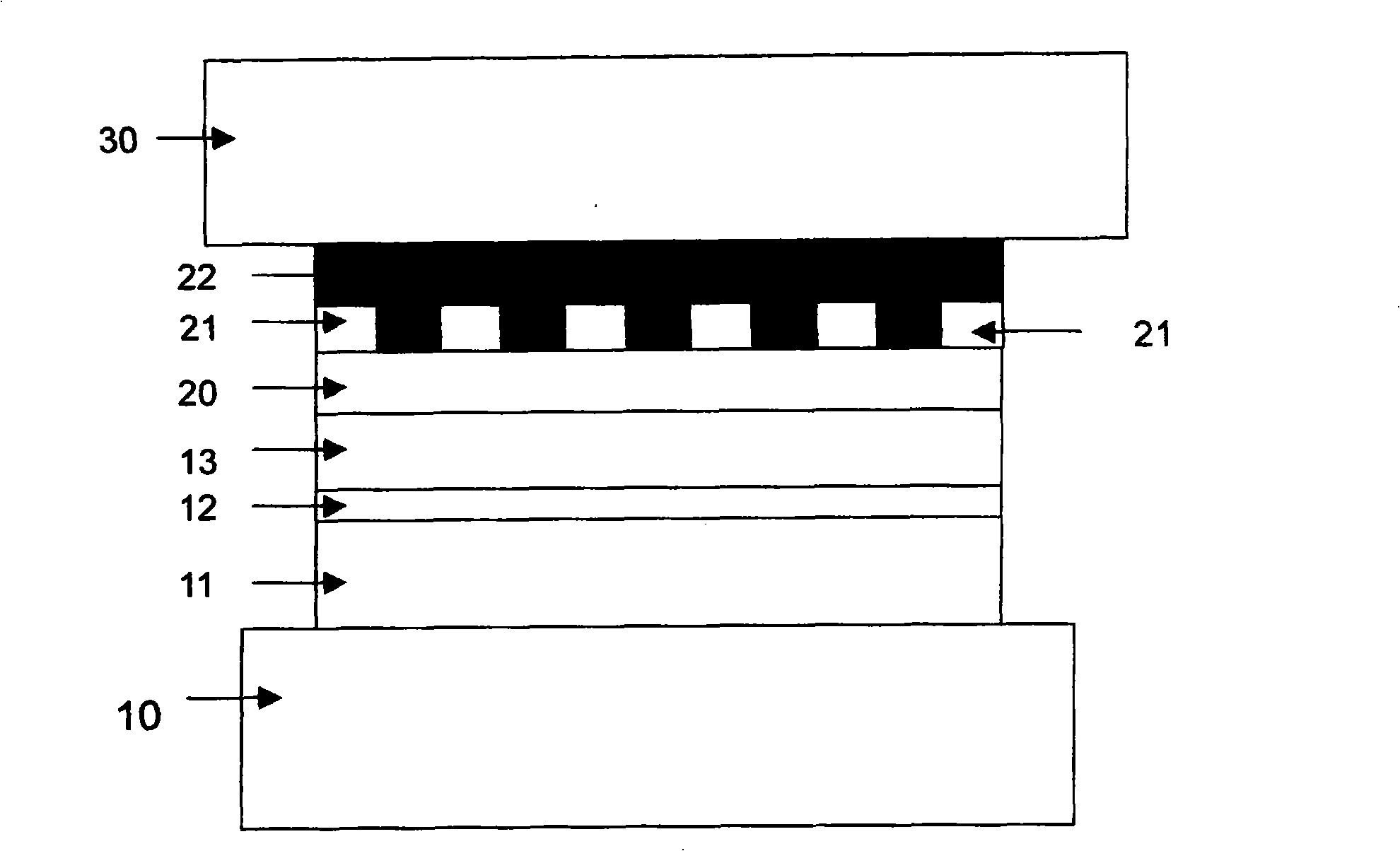
[0029] see Figure 1-Figure 4 As shown, a method for manufacturing a vertical structure light-emitting diode using an all-optical film system in the present invention comprises the following steps:

[0030] Step 1: Epitaxially grow GaN N-type contact layer 11, multi-quantum well active region 12 and GaN P-type contact layer 13 sequentially on substrate 10 by metal chemical organic vapor deposition method, the substrate 10 is sapphire Substrate;

[0031] Step 2: Use inductively coupled plasma, electron cyclotron resonance, and reactive ion etching dry etching techniques for device isolation;

[0032] Step 3: Fabricate an ITO optical film 20 on the GaN P-type contact layer 13 by electron beam evaporation technology;

[0033] Step 4: Make a layer of optical high-reflection film 21 on the ITO optical film 20 by using ion beam sputtering technology. The high-reflection film adopts a mesh structure, that is, part of the ITO optical film 20 is covered by the optical high-reflection...


PUM


Abstract

A method for preparing a light emitting diode (LED) with a vertical structure adopting an all optical film system. The method comprises the following steps: an N-type contact layer, an active area and a P-type contact layer are epitaxially grown in turn on a substrate; a device is isolated after etching; an ITO optical film is prepared on the P-type contact layer; an optical highly-reflective film is prepared on the ITO optical film, part area of which is exposed; metal films are prepared on the optical highly-reflective film and the exposed ITO optical film area so as to form a P electrode of the device; the insulated substrate is removed to expose the gallium nitride N-type contact layer; an ITO conductive optical reflection-reducing film is prepared on the surface of the gallium nitride N-type contact layer, and then undergoes surface roughening treatment; a metal electrode is prepared on the ITO conductive optical reflection-reducing film; a dielectric film is deposited on the surface of a chip so as to carry out surface passivation protection; and finally, the dielectric film in the metal electrode area is removed so as to carry out pressure welding and packaging, thereby completing the preparation of the device.

Description

technical field [0001] The invention belongs to the technical field of semiconductors, and is a method for manufacturing a vertical structure light-emitting diode using an all-optical film system, and is especially suitable for the production of a vertical structure and a self-supporting substrate with high efficiency. Background technique [0002] High-power GaN-based LEDs can be widely used in mobile device backlight, traffic signal display, automobile and other transportation vehicle lighting, outdoor full-color information display, landscape lighting, military lighting, LCD cup light source and other fields, with high photoelectric conversion efficiency , Green environmental protection, long life, fast response, rich colors, full solidification, small size and other advantages, it is another revolution in the history of human lighting after Edison invented the incandescent lamp. In the early 1990s, blue light-emitting diodes (LEDs) based on group III nitrides were succes...

Claims


Application Information

Patent Timeline
Patent Type & Authority Applications(China)
IPC IPC(8): H01L33/00
Inventor 伊晓燕王良臣王国宏李晋闽
Owner INST OF SEMICONDUCTORS - CHINESE ACAD OF SCI
Why Eureka
Try Eureka