Nonpolar GaN film and growth method thereof

A growth method and non-polar technology, applied in the field of non-polar GaN thin film and its growth, can solve the problems of reducing device efficiency, high cost, reducing luminous efficiency, etc., and achieve the effect of improving surface flatness

Active Publication Date: 2009-02-11
EPILIGHT TECH +2
View PDF0 Cites 4 Cited by
  • Summary
  • Abstract
  • Description
  • Claims
  • Application Information

AI Technical Summary

Problems solved by technology

The growth conditions are usually high temperature and high pressure, which is expensive and not conducive to commercialization. Therefore, most current applications are heterogeneous epitaxy on c-oriented sapphire.
A major disadvantage of using c-oriented sapphire is that its lattice mismatch with GaN film is as high as 13.6%. Although this shortcoming can be compensated by buffer layer technology, such a serious mismatch will still lead to a high density of defects in the epitaxial film , thereby reducing the device efficiency
In addition, GaN films are usually grown along the c-axis direction of its polar axis, and the strong built-in electric field generated by spontaneous polarization and piezoelectric effect greatly reduces the luminous efficiency.

Method used


Image

  • Nonpolar GaN film and growth method thereof
  • Nonpolar GaN film and growth method thereof

Examples


Embodiment Construction

[0015] Further illustrate the specific implementation steps of the present invention below in conjunction with accompanying drawing:

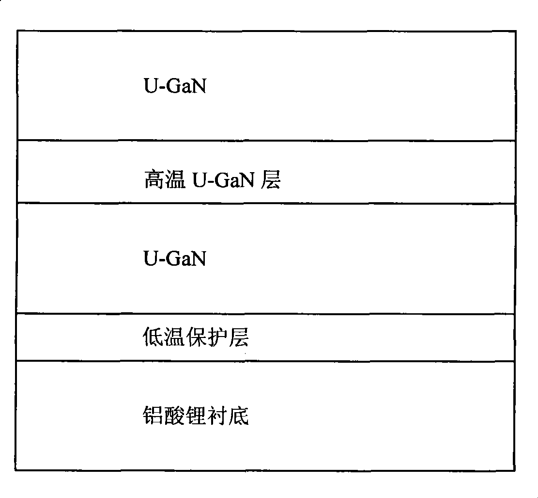
[0016] A non-polar GaN thin film, which is synthetically grown on a lithium aluminate substrate by using an MOCVD system. The thin film includes a low-temperature protective layer, a U-GaN layer, a high-temperature U-GaN layer and another a U-GaN layer.

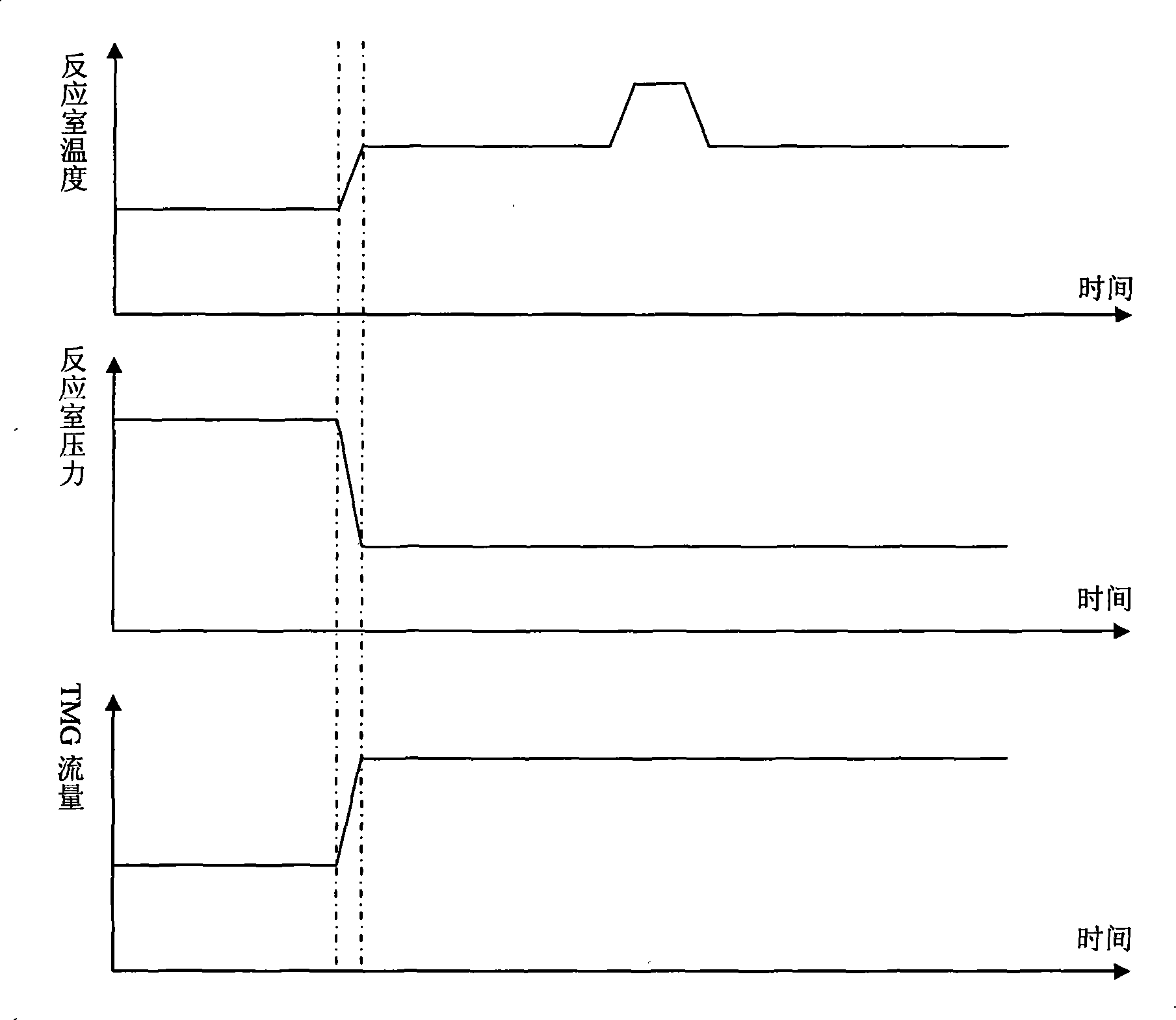
[0017] A kind of growth method of nonpolar GaN film, in MOCVD system, in N 2 Under protection, (in-situ heat treatment can be performed at 600-900°C or not) the temperature is raised to 800-900°C to grow a low-temperature protective layer. The pressure of the low-temperature protective layer is relatively high (150-500torr), and the TMGa flow rate is relatively low (1 -50sccm, corresponding to the molar flow rate: 4E-6mole / min—3E-4mole / min), then reduce the pressure (100-300torr), raise the temperature to 1000-1100°C to continue growing the U-GaN layer, and the TMGa flow rate is relatively hi...


PUM


Abstract

The invention provides a nonpolar GaN film and the growth method thereof. The method comprises the following steps: first, heating to a temperature of 800 DEG C to 900 DEG C and growing a low-temperature protective layer on a lithium aluminate (LiAlO2) substrate in a metal organic chemical vapor deposition (MOCVD) system under the protection of N2, wherein the pressure in the reaction chamber of the low-temperature protective layer is 150 to 500 torr, and the flow rate of trimethyl gallium (TMGa) is 1 to 50 sccm, and the molar flow rate corresponding to the flow rate is 4E-6mole/min to 3E-4mole/min; then, reducing the pressure to 100 to 300 torr, heating to 1000 DEG C to 1100 DEG C and proceeding with the growth of the undoped gallium nitride (U-GaN) layer, wherein the flow rate of TMGa is 10 to 200 sccm, and the corresponding molar flow rate thereof is 4E-5mol/min to 1E-3mole/min; further heating to 1150 DEG C to 1200 DEG C, and growing the high-temperature U-GaN for about 100 nm; and then further cooling to 1000 DEG C to 1100 DEG C and growing U-GaN. The growth of the low-temperature protective layer protects the LiAlO2 substrate against the damage caused by the high temperature, and the method aims to improve the surface smoothness of the grown GaN film by heating U-GaN to a high temperature for a short term.

Description

technical field [0001] The present invention relates to a novel substrate LiAlO 2 On the material, a non-polar GaN film and its growth method are grown on a mass-produced MOCVD machine. Background technique [0002] The new generation of semiconductor materials represented by GaN has attracted widespread attention due to its wide direct bandgap (Eg=3.4eV), high thermal conductivity, high hardness, high chemical stability, low dielectric constant, and radiation resistance. It has great application potential in the fields of solid-state lighting, solid-state lasers, optical information storage, and ultraviolet detectors. Calculated according to China's electricity consumption in 2002, if solid-state lighting is used to replace traditional light sources, the power generation of the Three Gorges Hydropower Station can be saved a year, which will have huge economic, environmental and social benefits; and according to the calculations of the US Department of Energy, by 2010, The...

Claims


Application Information

Patent Timeline
Patent Type & Authority Applications(China)
IPC IPC(8): H01L33/00H01S5/30H01L33/02
Inventor 周健华郝茂盛颜建锋潘尧波周圣明
Owner EPILIGHT TECH
Why Eureka
Try Eureka