Process for producing siliceous film and substrate with siliceous film produced thereby
A siliceous film, silicon substrate technology, applied in semiconductor/solid-state device manufacturing, gaseous chemical plating, coating, etc., can solve the problems of uneven etching rate, high etching rate, cracks, etc., and achieve excellent mechanical The effect of strength, uniform quality, uniform etch rate
- Summary
- Abstract
- Description
- Claims
- Application Information
AI Technical Summary
Problems solved by technology
Method used
Image
Examples
preparation example Construction
[0023] Preparation method of siliceous membrane
[0024] The preparation method of the siliceous film of the present invention can form a non-porous film with uniform film quality on the silicon substrate with concavities and convexities. The silicon film can thus be formed as a planarizing insulating film (premetal insulating film) for use in transistor elements or capacitor elements in electronic devices. In addition, a silicon film may be formed on a grooved silicon substrate to fill the groove, thereby forming a trench isolation structure. The present invention will be described in detail based on the method of forming the trench isolation structure.
[0025] In the method for preparing a siliceous membrane of the present invention, the process is performed according to the following steps to form a trench isolation structure:
[0026] An insulating film forming step of forming an insulating film having a hydrogen content of not less than 9×10 on the surface of a silicon...
Embodiment 1
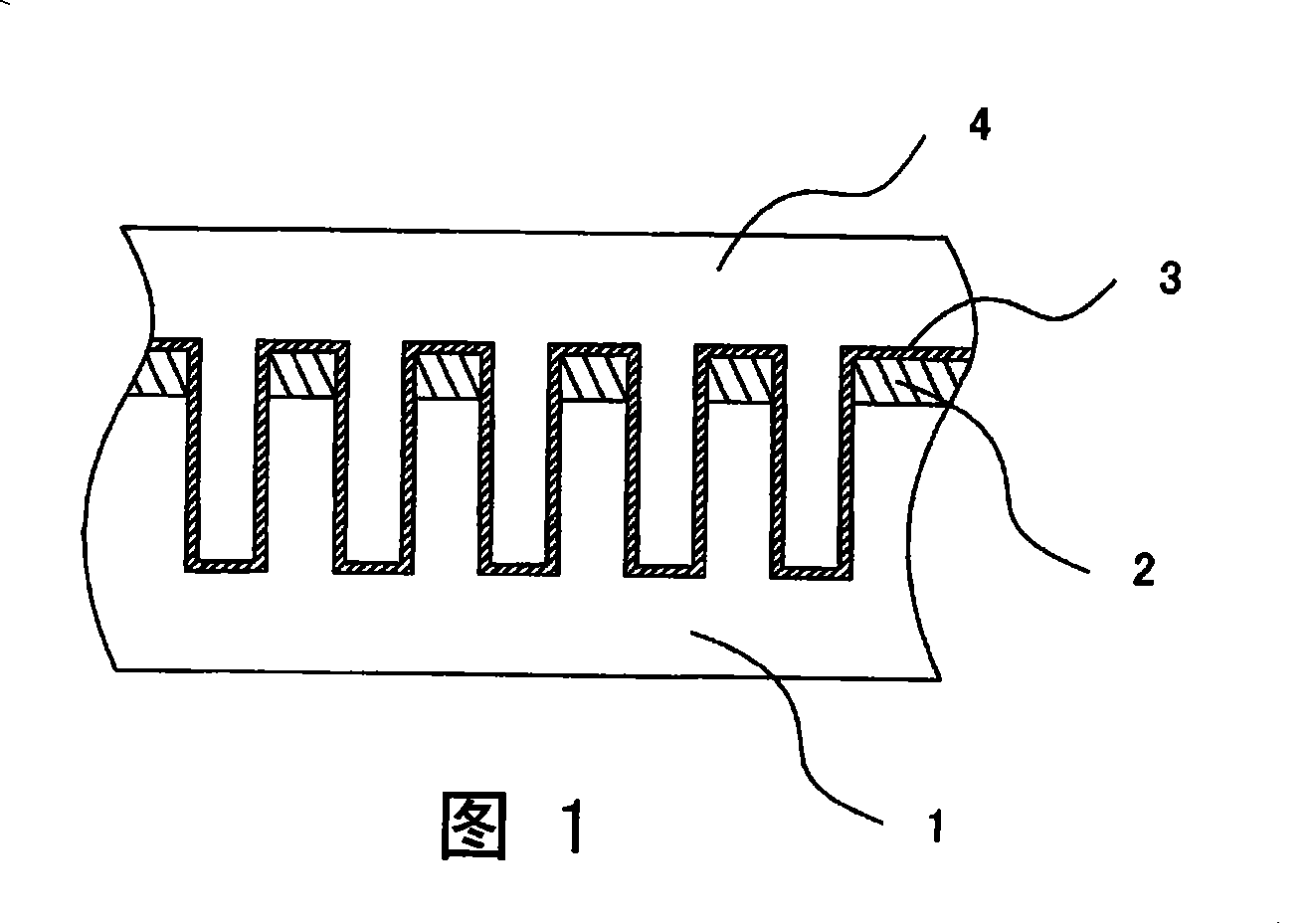
[0093] The present invention will be described in more detail with reference to the following embodiment, together with FIG. 1 , which discloses a contemplated technique for burying an element isolation trench STI (Shallow Trench Isolation) structure.
[0094] A grooved sample was first provided for evaluation of the configuration shown in FIG. 1 . A grooved sample (five grooves are shown in the figure) was formed by depositing a silicon nitride (SiN) film 2 to a thickness of 150 nm on the upper surface of a silicon substrate 1, followed by photolithography and dry etching. In this example, for all five grooves, the width is, for example, 80 nm to 400 nm, and the depth is, for example, 450 nm (the depth of the silicon substrate portion is 300 nm).
[0095] Using TEOS as a silicon source, a 20 nm-thick silicon dioxide film 3 was deposited on the grooved sample having the above-described structure by plasma chemical vapor deposition (plasma TEOS).
[0096] The silicon dioxide f...
Embodiment 2
[0104] Samples were prepared in the same manner as in Example 1, except that a 20 nm-thick silicon nitride film was deposited by plasma chemical vapor deposition (PE-CVD) instead of the plasma TEOS film shown in FIG. 1 .
[0105] The silicon nitride film 3 was formed by the above-mentioned PE-CVD under the following film-forming conditions. SiH 4 / NH 3 Gas flow rate and source power / bias power: SiH 4 / NH 3 = 55 / 110 sccm, SRF / BRF = 4400 / 2600W, substrate temperature = 400°C.
[0106] SIMS analysis and TDS measurements showed that the plasma PE-CVD film contained excess hydrogen. Specifically, according to SIMS analysis, the hydrogen content of the membrane is about 1 × 10 21 atms / cm 3 , according to TDS analysis, it was confirmed that hydrogen was released from the membrane in vacuum at a temperature of about 350 °C, indicating that the membrane contained hydrogen.
[0107] Film formation and heat treatment using the polysilazane solution were performed in the same manner...
PUM
| Property | Measurement | Unit |
|---|---|---|
| thickness | aaaaa | aaaaa |
| thickness | aaaaa | aaaaa |
| thickness | aaaaa | aaaaa |
Abstract
Description
Claims
Application Information


