Method for making nano lens array
A lens and nano technology, applied in the photoengraving process of lens and pattern surface, optics and other directions, can solve the problems of high production cost and long processing cycle of nano lens, and achieve low cost, controllable duty cycle and high efficiency. Effect
- Summary
- Abstract
- Description
- Claims
- Application Information
AI Technical Summary
Problems solved by technology
Method used
Image

Examples
Embodiment 1
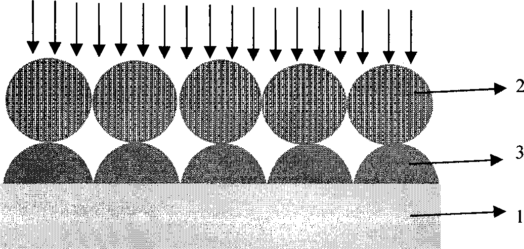
[0025] In this embodiment, fused silica is used as a substrate to fabricate a nanolens array with a diameter of 400 nm and a relief depth of 100 nm and 200 nm, respectively.
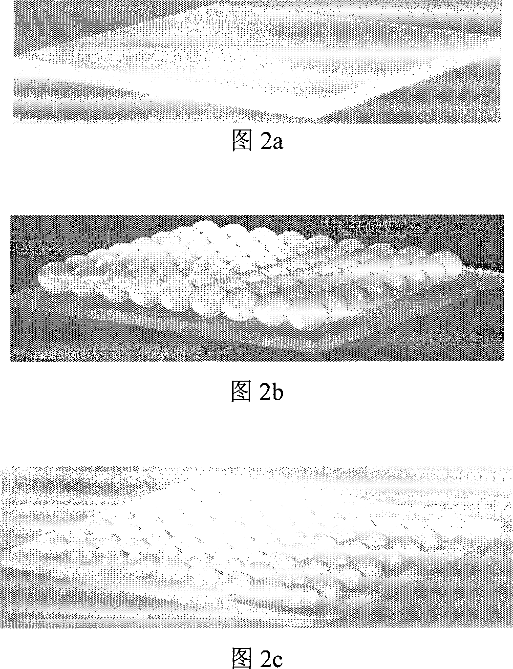
[0026] First, fused silica is used as the substrate, and the substrate is hydrophilized by chemical methods, such as figure 2 As shown in a; then 0.5μl of monodisperse polystyrene nanosphere hydrosol with a concentration of 3% and a diameter of 400nm is uniformly coated on the surface of the glass substrate, the solvent is slowly evaporated, and the colloidal spheres self-assemble into an array, such as figure 2 Shown in b; Reactive ion etching RIE is used to etch the self-assembled layer of polystyrene nanospheres to achieve the production of the required lens, such as figure 2 As shown in c; choose 1:1 etching rate ratio, adjust the etching power and reflection power and the flow of etching gas, control the etching rate of quartz at 20nm / min, after 5 minutes of etching, the formation period is 400nm, re...
Embodiment 2
[0028] In this embodiment, zinc selenide is used as the base to produce a nanolens array with a diameter of 6000 nm and a relief depth of 3000 nm; first, zinc selenide is used as the substrate, and the substrate is hydrophilized by a chemical method; then the concentration is 1%, and the diameter is 1%. 1.5μl of 8000nm polystyrene DVB copolymer particle suspension silicon microspheres are uniformly coated on the surface of the substrate to slowly evaporate the solvent, and the colloidal spheres self-assemble into an array; the polymer microspheres are self-assembled by inductively coupled plasma etching ICP The layer is etched, the etching rate ratio is controlled at 300nm / min, and the required lens is produced through 10min etching. The schematic diagram of the nanolens is shown as Figure 5 As shown, the diameter of the nano lens is 6000 nm, and the relief depth is 3000 nm.
Embodiment 3
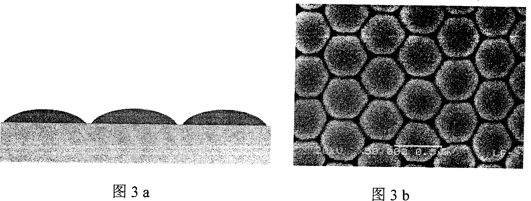
[0030] In this embodiment, silicon is used as a substrate to fabricate a nanolens array with a diameter of 200 nm and a relief depth of 50 nm. Using silicon as the substrate, the substrate is hydrophilized by chemical methods; 0.5μl of monodisperse polystyrene nanosphere hydrosol with a concentration of 1% and a diameter of 200nm is uniformly coated on the surface of the substrate to self-assemble to form an array; adopt 5 % Concentration of HF solution is wet-etched, and the result is obtained after 3 minutes Figure 6 Nano lens shown.
PUM
| Property | Measurement | Unit |
|---|---|---|
| Diameter | aaaaa | aaaaa |
| Depth | aaaaa | aaaaa |
| Diameter | aaaaa | aaaaa |
Abstract
Description
Claims
Application Information
 - R&D
- Intellectual Property
- Life Sciences
- Materials
- Tech Scout
- Unparalleled Data Quality
- Higher Quality Content
- 60% Fewer Hallucinations
Browse by: Latest US Patents, China's latest patents, Technical Efficacy Thesaurus, Application Domain, Technology Topic, Popular Technical Reports.
© 2025 PatSnap. All rights reserved.Legal|Privacy policy|Modern Slavery Act Transparency Statement|Sitemap|About US| Contact US: help@patsnap.com