Manufacturing method for vertical DMOS device

An oxide semiconductor and vertical double-diffusion technology, which is applied in semiconductor/solid-state device manufacturing, electrical components, circuits, etc., can solve the problems of cumbersome manufacturing process and high cost, so as to save manufacturing cost, reduce parasitic resistance, parasitic transistor The effect of weakening the effect

Inactive Publication Date: 2009-03-11
UNIV OF ELECTRONIC SCI & TECH OF CHINA
View PDF0 Cites 32 Cited by
  • Summary
  • Abstract
  • Description
  • Claims
  • Application Information

AI Technical Summary

Problems solved by technology

According to this manufacturing method, the manufacturing process is relatively cumbe

Method used


Image

  • Manufacturing method for vertical DMOS device
  • Manufacturing method for vertical DMOS device
  • Manufacturing method for vertical DMOS device

Examples


Embodiment Construction

[0034] The manufacturing method of a vertical double-diffused metal oxide semiconductor device of the present invention greatly saves the manufacturing cost of the device, and effectively weakens the parasitic transistor effect of the device.

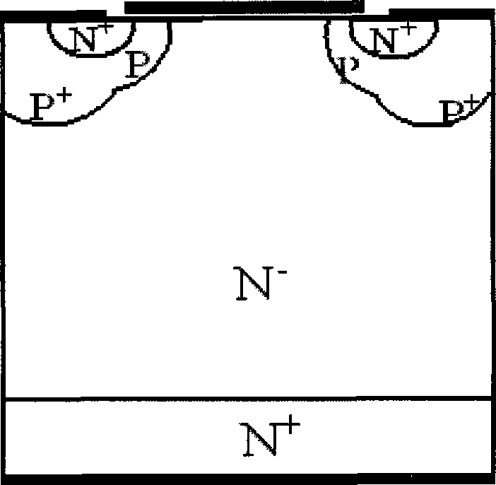
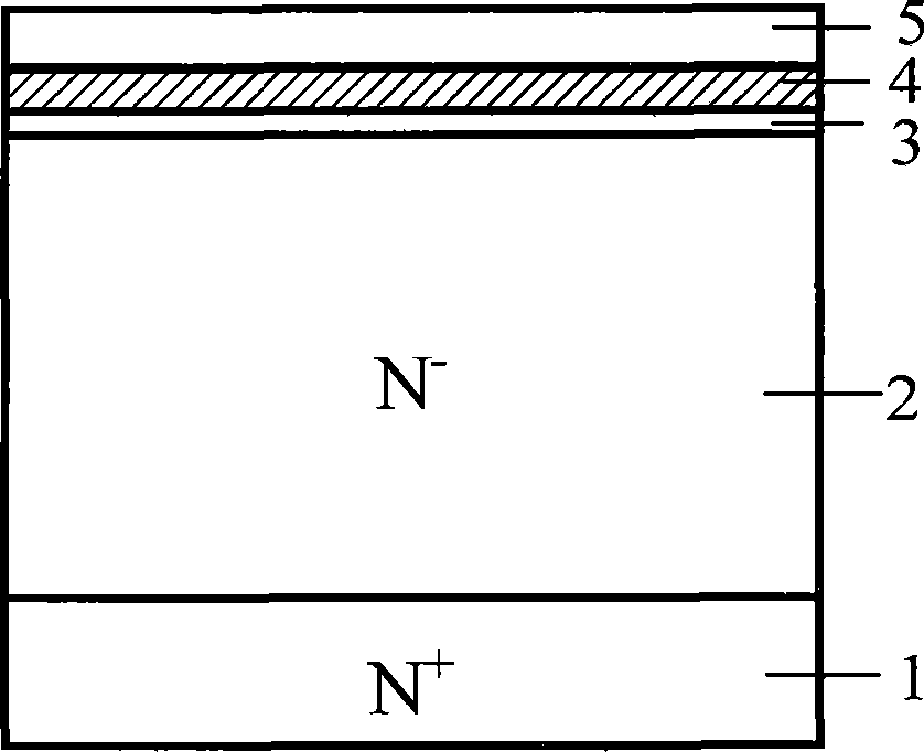
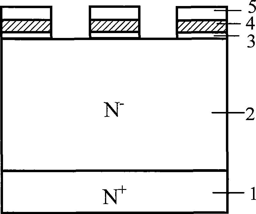
[0035] During specific implementation, for a low-voltage device, such as a 100V vertical double-diffused metal-oxide-semiconductor device, its specific implementation process includes: (1) in N + The growth concentration on the substrate was 1×10 15 cm -3 , with a thickness of 10 μmN - The epitaxial layer is then heated in an oxygen atmosphere at 1000°C for about 2 hours to grow an oxide layer of about 200nm, and then deposit polysilicon with a thickness of 800nm ​​by chemical vapor deposition, and do arsenic doping while depositing, and the concentration of arsenic doping for 10 20 cm -3 order, and then generate silicon dioxide of about 500nm by heating in an oxygen atmosphere at 1000°C for about 30 minutes; (2) through the mask of...


PUM


Abstract

The invention relates to a method for preparing a vertical double-diffusion metal oxide semiconductor device, which belongs to the technical preparation field of a semiconductor. The method comprises the main preparing steps: preparing a N<+> substrate, extending and growing N<->, oxidizing gate oxidation, depositing and adulterating polysilicon, depositing silicon dioxide, etching polysilicon windows, injecting and pushing a P trap, injecting high-concentration deep P<+>, injecting a N<+> source, oxidizing and forming a contact hole, etching a groove-shaped window by using an oxidizing layer as a mask, depositing metal, etching metal, passivating and back metalizing. The invention can manufacture a VDMOS device by only using two mask plates, the manufacturing cost of the device is greatly reduced, and meanwhile, the parasitic transistor effect of the device is weakened for the existence of a P<+> layer and the introduction of groove-shaped source contact metal, and the resistance among drain sources is reduced. The invention can be used for the production and the manufacture of the VDMOS device, other semiconductor devices (such as an insulating gate double-pole transistor) and an integrated circuit.

Description

technical field [0001] The invention relates to a method for manufacturing a vertical double-diffused metal oxide semiconductor (VDMOS) device, belonging to the field of semiconductor technology manufacturing. Background technique [0002] At present, the application fields of power devices are becoming wider and wider, and can be widely used in DC-DC converters, DC-AC converters, relays, motor drives, etc. The power vertical double-diffused metal oxide semiconductor has a higher operating frequency, and it is a voltage-controlled device, its driving current is very small, and the driving circuit is relatively simple, so its application range is wider. Power vertical double-diffused metal oxide semiconductors are an important basis for power electronics, and are often used in power integrated circuits and power integrated systems due to their high withstand voltage and high frequency characteristics. [0003] The traditional vertical double-diffused metal oxide semiconducto...

Claims


Application Information

Patent Timeline
IPC IPC(8): H01L21/336
Inventor 李泽宏钱梦亮连延杰张波
Owner UNIV OF ELECTRONIC SCI & TECH OF CHINA
Why Eureka
Try Eureka