Preparation for copper-indium-galliun-selenium-sulfur or copper-indium-galliun-selenium or copper-indium-galliun-sulfur film solar cell absorption layer

A copper indium gallium selenide sulfur, solar cell technology, applied in coatings, circuits, electrical components and other directions, can solve the problems of poor safety, difficult transportation and storage, high price, etc., to increase the scope of application and avoid highly toxic gases , the effect of improving the efficiency of use

Inactive Publication Date: 2009-03-11
苏州富能技术有限公司
View PDF0 Cites 29 Cited by
  • Summary
  • Abstract
  • Description
  • Claims
  • Application Information

AI Technical Summary

Problems solved by technology

However, due to the use of highly toxic hydrogen selenide and hydrogen sulfide during selenization and/or sulfidation, the gas is flammable and explosive, has poor safety, is expensive, difficult to transport and store, and is

Method used


Image

  • Preparation for copper-indium-galliun-selenium-sulfur or copper-indium-galliun-selenium or copper-indium-galliun-sulfur film solar cell absorption layer
  • Preparation for copper-indium-galliun-selenium-sulfur or copper-indium-galliun-selenium or copper-indium-galliun-sulfur film solar cell absorption layer

Examples


specific Embodiment 1

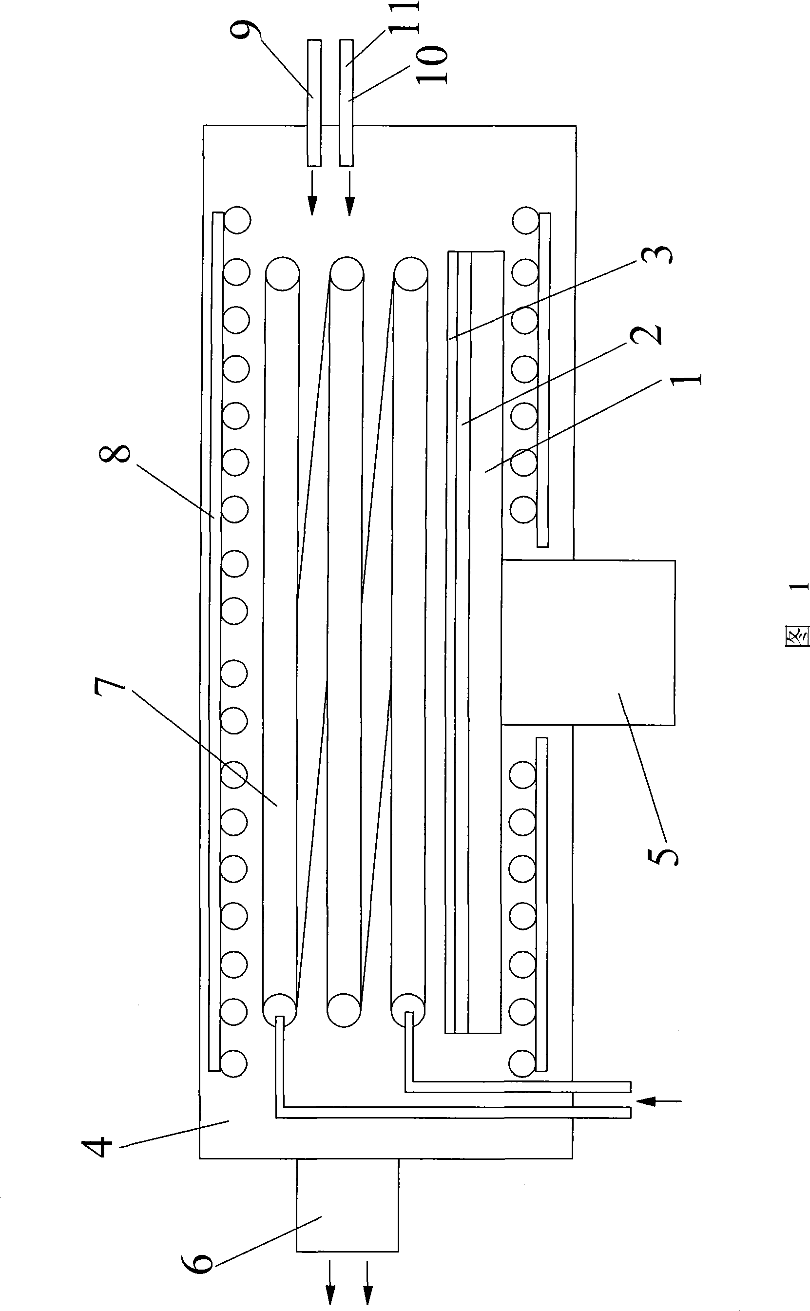
[0034] A method for preparing an absorber layer of a copper indium gallium selenide thin film solar cell, comprising the following steps:

[0035] 1) Prepare the underlying conductive film: on the substrate 1, use mask evaporation or sputtering to form the underlying metal conductive film 2;

[0036] 2) Preparing the metal precursor film 3 of the thin-film battery: plating the metal precursor film 3 of copper, indium, and gallium on the underlying conductive film 2 by magnetron sputtering or vacuum evaporation;

[0037] 3) Selenization reaction: place the module to be processed in the reaction vessel 4, then evacuate the reaction vessel 4 into a vacuum state, and fill the reaction vessel 4 with a protective gas that does not react with copper, indium, and gallium to achieve a certain vacuum degree, for example: 1×10 -1 After the vacuum degree of Pa, carry out heating and plasma discharge in the reaction vessel, the heating can choose a value between 200~600 ℃ (for example, wh...

specific Embodiment 2

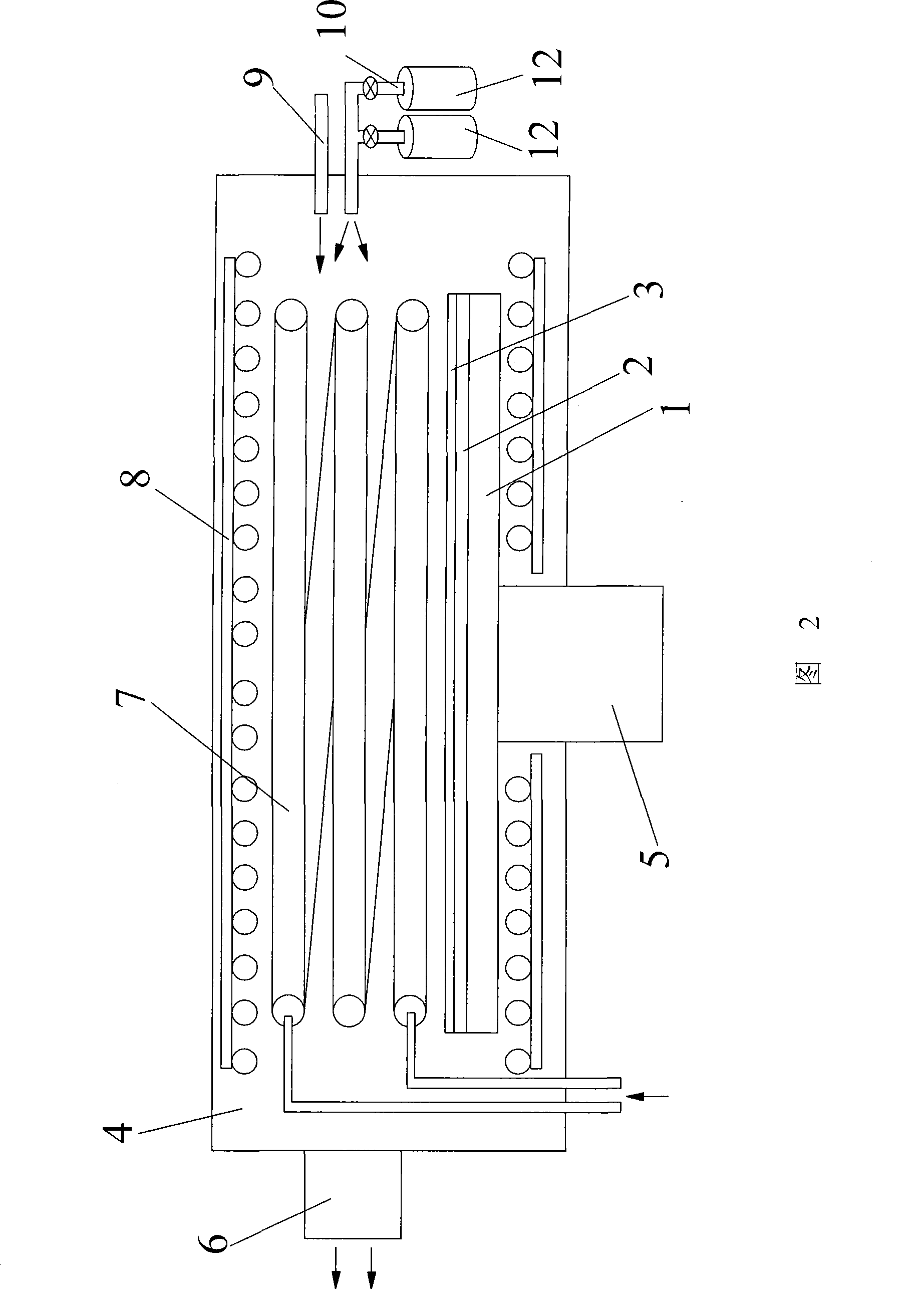
[0041] A method for preparing an absorber layer of a copper indium gallium sulfide thin film solar cell: using organometallic sulfur to replace the organometallic selenium in the first embodiment, and the other being the same as the first embodiment, to obtain an absorber layer of a copper indium gallium sulfide thin film solar cell.

specific Embodiment 3

[0042] A preparation method for the absorbing layer of a copper indium gallium selenide sulfur thin film solar cell: use organic metal sulfur and organic metal selenium to replace the organic metal selenium in the first embodiment, and the other is the same as the first embodiment to obtain a copper indium gallium selenide sulfur thin film solar cell battery absorber.


PUM


Abstract

The invention discloses a preparation method for a CIGSeS, CIGSe or CIGS thin-film solar cell absorption layer. After a base conductive film and a metal precursor film are prepared in sequence, a selenylation and/or sulfurization reaction source is excited into free or ionized selenium molecules and/or sulfur molecules in vacuum due to high temperature and plasma discharge, and then selenylation and/or sulfurization reaction is carried out on the metal precursor film. The invention also discloses coating equipment of a CIGSeS, CIGSe or CIGS thin-film solar cell absorption layer which comprises a reaction vessel and a vacuum pump arranged outside the reaction vessel and communicated with the reaction vessel, wherein a rotating axle with an upper end extended into inside the reaction vessel is arranged under the reaction vessel, a plasma generator and a heating device are also arranged in the reaction vessel, and the reaction vessel is also provided with a shielding gas input device and a selenylation and/or sulfurization reaction source device in a communicating way. The invention can keep higher conversion efficiency of the original method, also avoids the use of highly toxic gas such as hydrogen selenide or hydrogen sulphide, enhances the security of coating processing, and also improves the use efficiency of the selenium source and/or the sulfur source.

Description

technical field [0001] The invention relates to a preparation method and coating equipment of a copper indium gallium selenide sulfur or copper indium gallium selenide or copper indium gallium sulfur thin film solar cell absorption layer. Background technique [0002] The existing copper indium gallium selenide sulfur (CuInGaSeS) or copper indium gallium selenide (CuInGaSe) or copper indium gallium sulfur (CuInGaS) thin film solar cell preparation methods are divided into two categories: the first category is called multiple co-evaporation method , the second category is called selenization and / or sulfurization. The multi-component co-evaporation method is characterized by simultaneous evaporation of four components of copper, indium, gallium, and selenium (or sulfur), or first plating indium, gallium, and selenium, then copper, selenium, and finally plating indium, gallium, and selenium in three stages Law. The co-evaporation method is characterized by large film crystals...

Claims


Application Information

Patent Timeline
IPC IPC(8): H01L31/18C23C14/06C23C14/24C23C14/35
CPCY02P70/50
Inventor 刘穆清窦晓明唐健范滨
Owner 苏州富能技术有限公司
Why Eureka
Try Eureka