Field effect transistor device with graphene as electrode and method for producing the same

A technology of field-effect transistors and graphene, which is applied in the direction of electrical solid-state devices, semiconductor/solid-state device manufacturing, semiconductor devices, etc., to achieve the effects of size reduction, high response sensitivity, and high application value

Inactive Publication Date: 2009-04-08
PEKING UNIV
View PDF0 Cites 19 Cited by
  • Summary
  • Abstract
  • Description
  • Claims
  • Application Information

AI Technical Summary

Problems solved by technology

However, so far, there are few reports on graphene as a two-dimensional electrode

Method used


Image

  • Field effect transistor device with graphene as electrode and method for producing the same
  • Field effect transistor device with graphene as electrode and method for producing the same
  • Field effect transistor device with graphene as electrode and method for producing the same

Examples


Embodiment 1

[0026] Embodiment 1, preparation nanoscale field effect transistor device

[0027] The preparation method of the nanoscale field effect transistor device comprises the following steps:

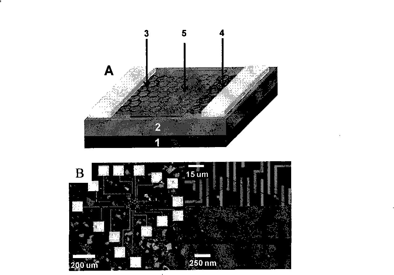
[0028] 1) On a heavily doped silicon substrate containing a layer of 300nm thick silicon dioxide, graphite without any processing is placed on the substrate and peeled off repeatedly to obtain graphene;

[0029] 2) Patterning graphene by electron beam etching method;

[0030] 3) cover the patterned graphene obtained in step 2) with a metal mask, and utilize thermal evaporation method to obtain Cr layer and Au layer (5 nanometers / 40 nanometers) successively on the silicon substrate surface, and Au / Cr is used as the metal source and drain regions.

[0031] 4) A layer of PMMA (950, A2) was spin-coated on the surface of the above-mentioned transistor, the spin-coating rate was 4000PRM, the spin-coating time was 45s, and then dried at 170° C. for 2 minutes. Using an electron beam etching method,...

Embodiment 2

[0037] Embodiment 2, preparation nanoscale field effect transistor device

[0038] The preparation method of the nanoscale field effect transistor device comprises the following steps:

[0039] 1) On a heavily doped silicon substrate containing a layer of 300nm thick silicon dioxide, graphite without any processing is placed on the substrate and peeled off repeatedly to obtain graphene;

[0040] 2) Patterning graphene by electron beam etching method;

[0041] 3) cover the patterned graphene obtained in step 2) with a metal mask, and utilize thermal evaporation method to obtain Cr layer and Au layer (5 nanometers / 40 nanometers) successively on the silicon substrate surface, and Au / Cr is used as the metal source and drain regions.

[0042] 4) After spin-coating (4000PRM, 45s) a layer of PMMA (950, A2) on the surface of the above-mentioned transistor, dry it at 170° C. for 2 minutes. Using an electron beam etching method, the DesignCAD file is run on a computer to etch the pat...


PUM

PropertyMeasurementUnit
Concentrationaaaaaaaaaa
Widthaaaaaaaaaa
Thicknessaaaaaaaaaa

Abstract

The invention provides a field effect transistor device by taking graphene as an electrode and a preparation method thereof. In the device, the material of a source region and a drain region is graphene; the materials of a channel region are various small organic molecules, high polymers and semiconducting polymer materials, such as polythiophene, pentacene, polycyclic aromatic hydrocarbon, perylene imide and the like; and the material of a gate region is highly doped conductive silicone. The device further comprises a gate dielectric layer the material of which is silicon dioxide, silicon nitride and various high-K dielectrics. The nano field effect transistor device can be n-typed, p-typed or amphoteric type, and the device realizes all functions of a macroscopic field effect transistor device at the nanometer level. The transistor device has very high application value in terms of ultrasensitive environmental stimuli response devices, ultrasensitive solar stimuli response devices and the like. In addition, in the fields of molecular electronics and nanometer, the transistor device plays an essential role of promoting the development of ultramicro photoelectric devices with various dimensions at molecular level.

Description

technical field [0001] The invention relates to a field effect transistor device and a preparation method thereof, in particular to a field effect transistor device with graphene as an electrode and a preparation method thereof. Background technique [0002] As the size of traditional silicon-based transistors is gradually miniaturized to the molecular scale, a lot of research work has been done on nanoscale transport junctions, and it is expected to be able to characterize the electrical properties of single or several organic molecules. The ultimate goal in the field of nanoelectronics and molecular electronics is to obtain single-molecule or single-atom transistors. In principle, single-molecule-scale transistor devices can overcome the low carrier concentration defects of semiconductor materials and exhibit good field-effect transistor properties. To achieve this ultimate goal, it is crucial to prepare new materials, develop new device structures, and new methods of par...

Claims


Application Information

Patent Timeline
IPC IPC(8): H01L51/05H01L51/30H01L51/40
Inventor 郭雪峰曹阳杨凌春
Owner PEKING UNIV
Why Eureka
Try Eureka