
Method for preparing NiO transparent conductive film by two steps

A technology of transparent conductive film and film, applied in the direction of ion implantation plating, coating, metal material coating process, etc., can solve the problem of reducing the conductivity and optical transmittance of NiO transparent conductive film, and the carrier mobility in the film Reduced, many film defects, etc.

Inactive Publication Date: 2009-04-22
CHANGCHUN UNIV OF SCI & TECH
View PDF0 Cites 9 Cited by
  • Summary
  • Abstract
  • Description
  • Claims
  • Application Information

AI Technical Summary

Problems solved by technology

As far as the second type is concerned, although the ratio of Ni atoms and O atoms in the prepared NiO transparent conductive film can be adjusted in a wide range by controlling the flow rate of the oxidizing gas and the sputtering power during sputtering, this kind of This method has the problem of poor crystallization quality of the film, which is caused by its low-temperature growth characteristics, that is to say, there are more defects in the film under low-temperature growth, which reduces the carrier mobility in the film and greatly reduces the transparency of NiO. Conductivity and Optical Transmittance of Conductive Films

Method used


Image

  • Method for preparing NiO transparent conductive film by two steps
  • Method for preparing NiO transparent conductive film by two steps

Examples


Embodiment Construction

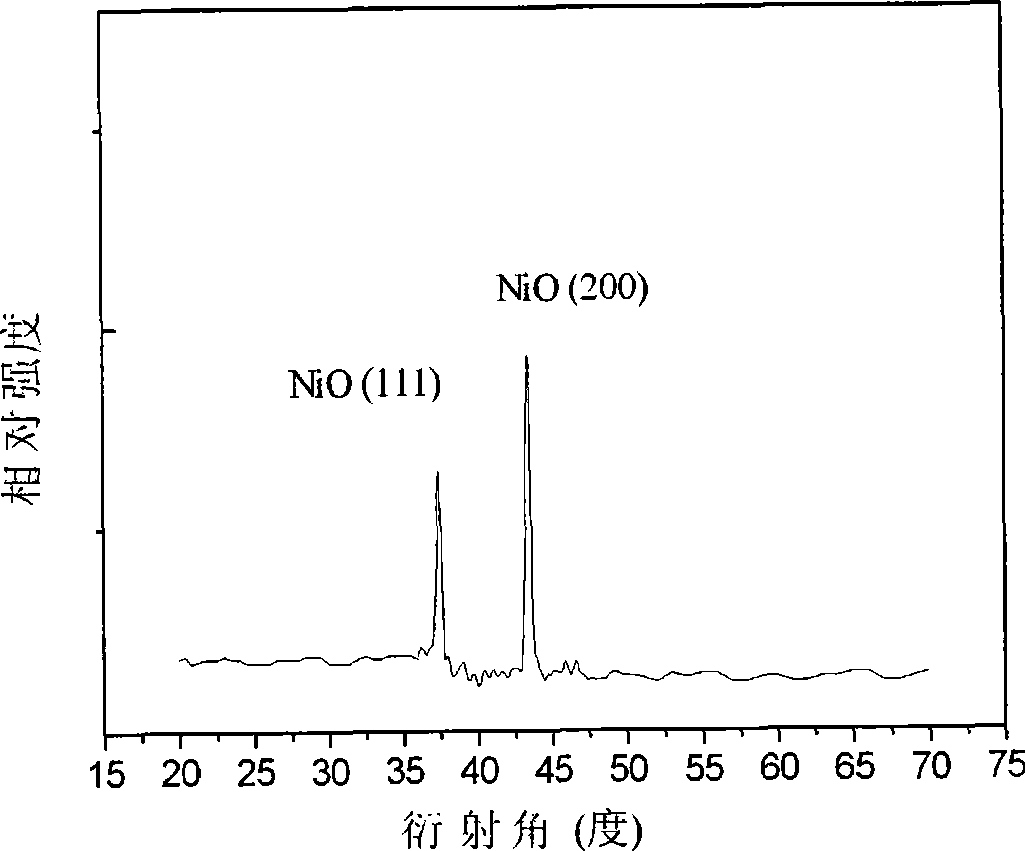
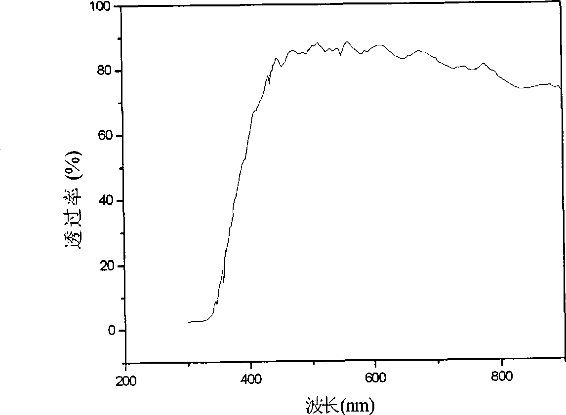
[0007] After cleaning the substrate, put it into a magnetron sputtering vacuum chamber, and adjust the distance between the Ni target and the substrate within the range of 5-10 cm. Then the Ni film is prepared by sputtering the Ni target, the sputtering time is 30-60 minutes, the sputtering power is 100-200W, the substrate is always kept at the same temperature, that is, a certain temperature in the range of 25-500°C, and the sputtering gas is a single Argon. Then, the substrate coated with the Ni film is placed in a high-temperature oxidation furnace, and oxygen is introduced at a flow rate of 5-15 l / min. The temperature of the high-temperature oxidation furnace is raised to a temperature in the range of 500-1200°C at a heating rate of 3-8°C / min, the thermal oxidation time is 30-180 minutes, and then the high temperature is lowered at a cooling rate of 2-8°C / min. The temperature of the oxidation furnace is lowered to room temperature.

[0008] Below is a specific example. ...


PUM


Abstract

The invention relates to a method for preparing a NiO transparent conductive film through two steps and belongs to the technical field of semiconductor optoelectronic material manufacture. The prior method adopts a complicated process for preparing a NiO ceramic target; and the NiO ceramic target is expensive and is easy to damage. In the process of preparing the NiO ceramic target by the prior method, the proportion of Ni atoms and O atoms is fixed so as to limit the adjusting range of the proportion of the Ni atoms and the O atoms in the prepared NiO transparent conductive film, thereby failing to meet difficult application requirements. Due to low-temperature growth, the film has more disadvantages, thereby causing the reduction of the mobility ratio of a current carrier in the film and greatly reducing the conductivity and the optical transmissivity of the NiO transparent conductive film. In step one of the method, a Ni film is prepared through sputtering the Ni target; and in step two, the obtained Ni film is positioned in an oxidation atmosphere, wherein the temperature is between 500 and 1,200 DEG C, the flow rate of oxygen gas is between 5 and 15 l / min, and time for thermal oxidization is between 30 and 180 minutes; and the Ni film is oxidized to form the NiO transparent conductive film.

Description

technical field [0001] The invention relates to a method for preparing a NiO transparent conductive film by magnetron sputtering, and belongs to the technical field of semiconductor optoelectronic material manufacturing. Background technique [0002] NiO transparent conductive film is a p-type, wide bandgap, transparent oxide semiconductor film material with transparent conductivity, electrochromic, gas detection, ultraviolet light detection and other properties, used in various flat-panel displays, solar cells, light-emitting diodes , in the ultraviolet light detector. The existing preparation method close to the present invention is the magnetron sputtering method, in which the sputtering target substance is sputtered onto the substrate by means of the magnetron sputtering to form a thin film. It is further divided into two types, one is to use NiO ceramic target as sputtering target, and use the plasma generated by argon glow discharge to sputter into film; the other is ...

Claims


Application Information

Patent Timeline
IPC IPC(8): C23C14/34C23C14/58C23C14/14C23C14/54
Inventor 王新李野王国政姜德龙付申成端木庆铎吴奎
Owner CHANGCHUN UNIV OF SCI & TECH
Learn More