Electroconductive particle placement sheet and anisotropic elctroconductive film

一种导电颗粒、薄片的技术,应用在导电连接、导电粘合剂、薄膜/薄片状的粘合剂等方向,能够解决连接缺陷、导电颗粒易于脱落、绝缘膜薄膜化限制等问题,达到绝缘性高、连接可靠性优异的效果

Active Publication Date: 2009-05-13
DEXERIALS CORP
View PDF5 Cites 42 Cited by
  • Summary
  • Abstract
  • Description
  • Claims
  • Application Information

AI Technical Summary

Problems solved by technology

However, if the film thickness of the insulating film becomes thinner, conductive particles tend to fall off during the manufacturing process or during use, causing connection defects, and there is a limit to the thinning of the insulating film

Method used


Image

  • Electroconductive particle placement sheet and anisotropic elctroconductive film
  • Electroconductive particle placement sheet and anisotropic elctroconductive film
  • Electroconductive particle placement sheet and anisotropic elctroconductive film

Examples


Embodiment 1

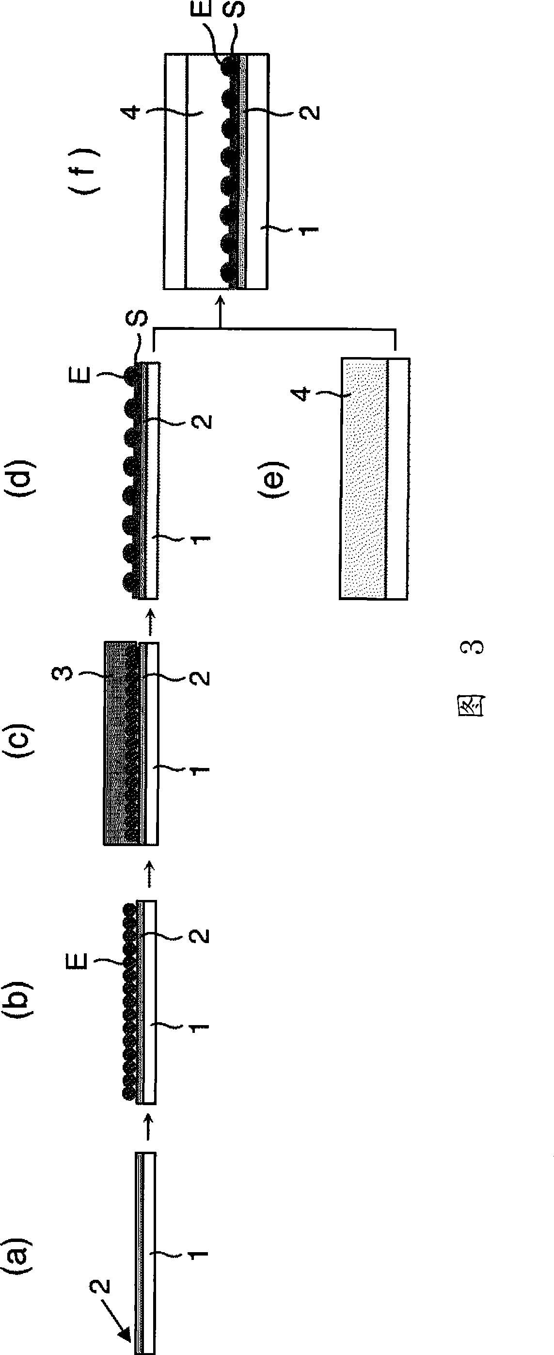
[0137]Mixed phenolic oxygen resin (manufactured by InChem, trade name: PKHC) 80 parts by mass, bisphenol A type liquid epoxy resin (manufactured by Asahi Kasei Chemical Co., Ltd., trade name: AER2603) 20 parts by mass, silane coupling agent (Japan Unicar Made by the company, trade name: A-187) 0.25 parts by mass, ethyl acetate 300 parts by mass, to obtain a varnish for an insulating resin sheet. The melt viscosity at 180° C. of the insulating resin sheet obtained by removing the solvent from the insulating resin sheet with varnish was 1500 Pa·s.

[0138] An acrylic polymer diluted with ethyl acetate to 5% by mass of the resin component was coated onto a 100 μm non-stretched copolymer polypropylene film using a knife coater, and dried at 80° C. for 10 minutes to form an adhesive layer with a thickness of 1 μm. The acrylic polymer used here is to use azobisisobutyronitrile as initiator, 62 mass parts of methyl acrylate, 30.6 mass parts of 2-ethylhexyl acrylate, 7 mass parts of 2...

Embodiment 2

[0150] As the insulating resin sheet, a phenolic resin (manufactured by InChem Corporation, trade name: PKHB, melt viscosity at 180° C. is 980 Pa·s) was used alone, the average particle diameter of the conductive particles was changed to 3 μm, and the filling rate was changed to 82%. Otherwise, a conductive particle-filled sheet was obtained in the same manner as in Example 1, and a conductive particle-arranged sheet (referred to as a conductive particle-arranged sheet B) was obtained in the same manner as in Example 1 except that the draw ratio was 2.7 times.

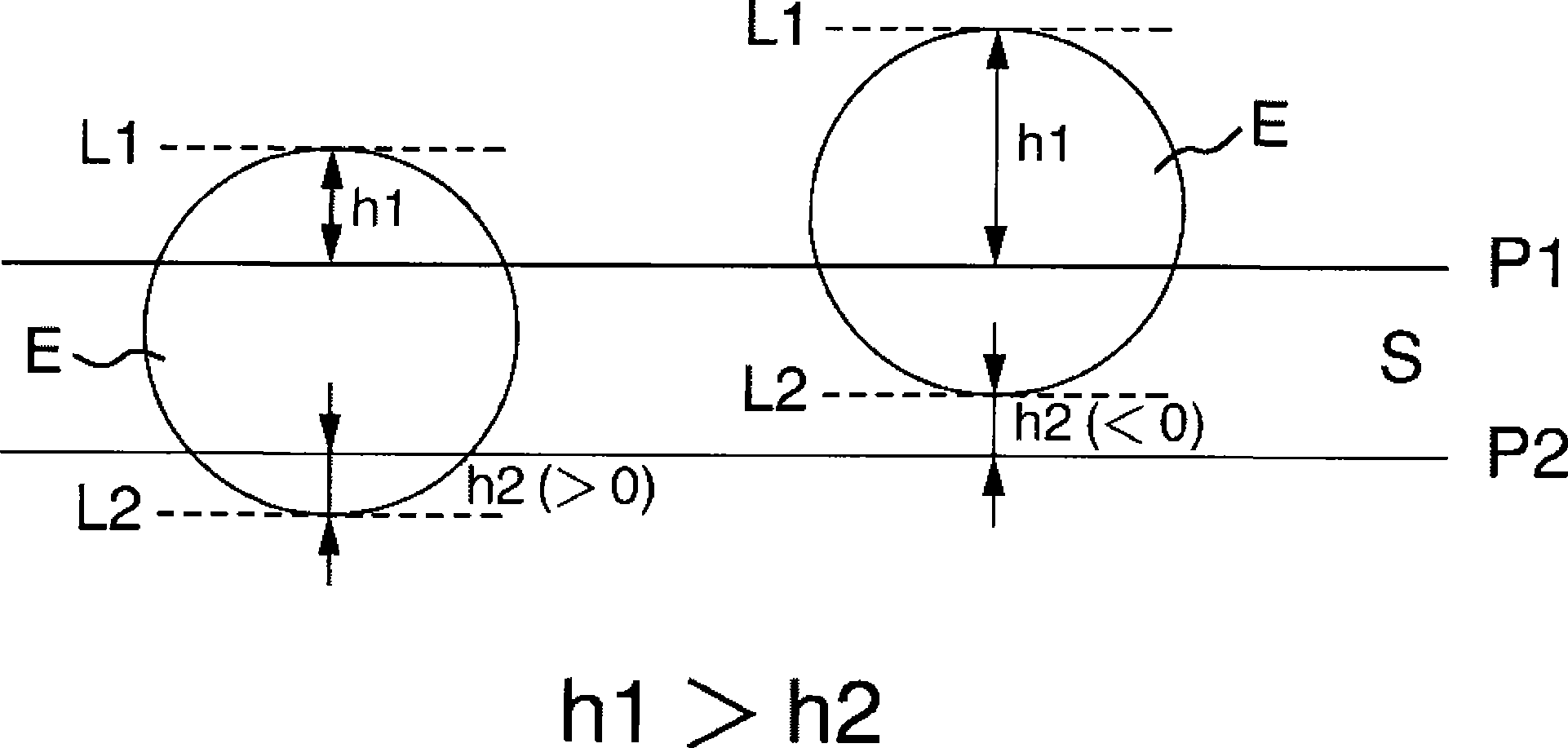
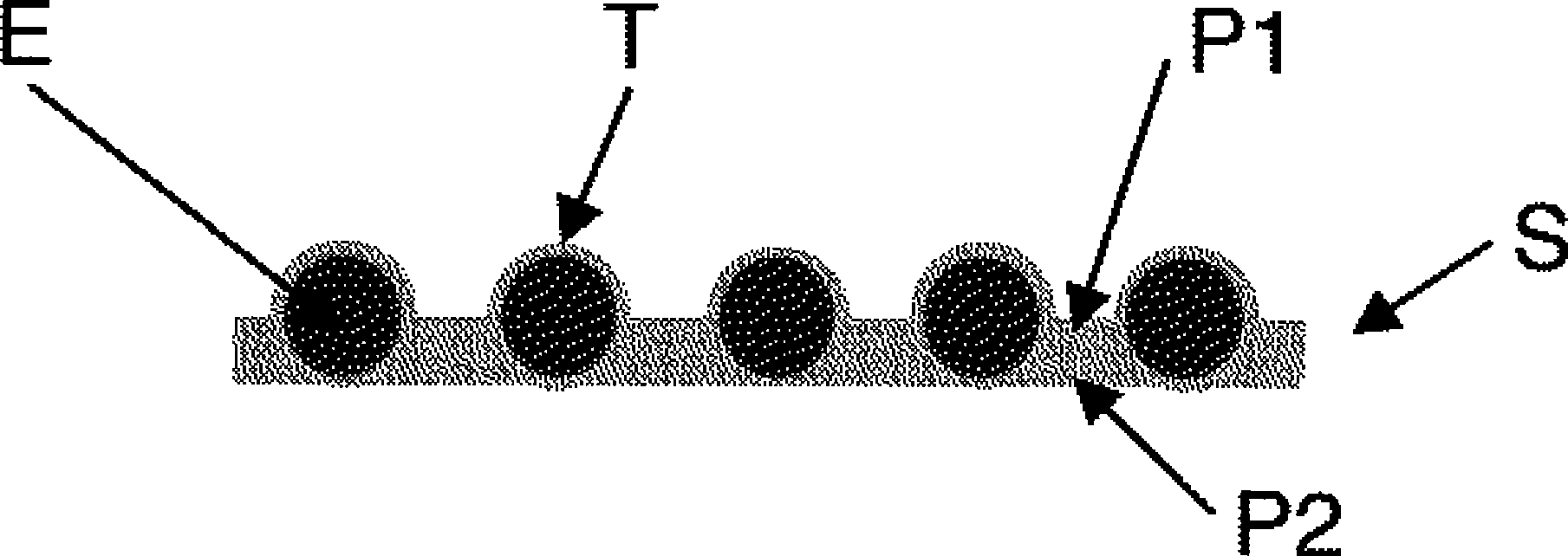
[0151] When the obtained conductive particle arrangement sheet B was observed using a scanning electron microscope, the conductive particles were present in the insulating resin sheet, the portion of the insulating resin sheet without conductive particles was approximately smooth, and the conductive particles protruded greatly on one side of the insulating resin sheet. Its protruding portion is covered with an insulatin...


PUM

PropertyMeasurementUnit
particle diameteraaaaaaaaaa

Abstract

This invention provides an electroconductive particle placement sheet comprising electroconductive particles and an insulating resin sheet. The thickness of the insulating resin sheet is smaller than the average particle diameter of the electroconductive particles. Electroconductive particles are protruded from the reference plane (P1) on at least one side of the insulating resin sheet. The electroconductive particle in is part protruded from the reference plane (P1) is covered with a layer formed of the same resin as in the insulating resin sheet. The electroconductive particle placement sheet is characterized by satisfying a relationship of h1 > h2 wherein h1 represents an average protrusion height, which is the average of distance between the reference plane (P1) and a tangential line (L1), which is a tangential line parallel to the reference plane (P1) of the electroconductive particle and is in contact with the part protruded from the reference plane (P1), and h2 represents an average protrusion height which is the average of distance between the reference plane (P2) and a tangential line (L2), which is a tangential line parallel to the reference plane (P2) of the electroconductive particle and is on the side opposite to the tangential line (L1), provided that, when the tangential line (L2) is within the insulating resin sheet, h2 < 0; when the tangential line (L2) is on the reference plane (P2), h2 = 0; and when the tangential line (L2) is outside the insulating resin sheet, h2 > 0.

Description

technical field [0001] The present invention relates to a conductive particle-arranged sheet useful as a connection element used between circuit boards or for connecting electronic components such as semiconductor chips to a circuit board. Background technique [0002] As a connection element for easy connection between a liquid crystal display and a semiconductor chip or TCP (TapeCarrier Package), between an FPC (Flexible Printed Circuit) and a TCP, or between an FPC and a printed circuit board, conductive particles are dispersed in an insulating Anisotropic Conductive Films in Sexual Adhesives. For example, anisotropic conductive films are widely used for connection between liquid crystal displays and control ICs of notebook personal computers or mobile phones, and are also used for flip chips in which semiconductor chips are directly mounted on printed circuit boards or flexible circuit boards. Encapsulation (Patent Documents 1, 2 and 3). [0003] In recent years, in th...

Claims


Application Information

Patent Timeline
Patent Type & Authority Applications(China)
IPC IPC(8): H01R11/01H01L21/60H05K3/32C09J7/22C09J7/30
CPCH01L2924/01015H05K2201/10378H01L2924/01046C09J2201/602H01L2924/0105H01L2924/01082H01L2924/0781H01L2924/01049H05K2201/10234H01L2224/83101H01L2224/16C08K7/18H01L2924/01019H01L2224/13144H01L2924/01029H01L2924/01027C09J2203/326H01L2924/014H01L2924/01013H01L24/28H01L2924/0665H01L2924/0103H01L24/27H01L2224/2919H01L2924/01047H01L2924/01079H01L2224/838H01L2924/14H01L24/83H01L24/29H01L2924/01005H01L2924/01033H01L2924/01006C09J2205/106H01L2924/01078H05K3/323C09J7/0239H01L2924/07802H01L2924/15788C09J7/22C09J7/30Y10T156/10Y10T428/2495C09J2301/314C09J2301/41H01L2924/00C09J9/02C09J11/04
Inventor 臼井健敏岛田仁
Owner DEXERIALS CORP
Why Eureka
Try Eureka