Cell electrofusion chip and method for manufacturing the same

An electrofusion and cell technology, applied in biochemical equipment and methods, tissue cell/virus culture devices, stress-stimulated microbial growth methods, etc. Weak oxidation ability, poor visibility enhancement, etc., to achieve the effect of improving electric field inductive force, improving chemical corrosion resistance, and good optical visibility

Inactive Publication Date: 2009-05-20
ARMY MEDICAL UNIV
View PDF0 Cites 2 Cited by
  • Summary
  • Abstract
  • Description
  • Claims
  • Application Information

AI Technical Summary

Problems solved by technology

[0005] As the core component of a complete cell electrofusion system, the cell fusion chip has higher and higher requirements for its structure and manufacturing process. However, in general, there are currently few domestic research and development of cell electrofusion chips, mainly as follows: Defects: The electric field strength and electric field gradient generated by the microelectrode are weak, and more precise control cannot be achieved; it is poor in enhancing the degree of visualization, and it is not easy (or the effect is not good) to observe the process of cell electrofusion inside the chip, which is not conducive to cell electrofusion Observe and record the cells in real time during the process, which is inconvenient to manipulate the cells
And in the selection of processing materials, there are also problems of weak corrosion resistance and oxidation resistance of materials.

Method used


Image

  • Cell electrofusion chip and method for manufacturing the same
  • Cell electrofusion chip and method for manufacturing the same
  • Cell electrofusion chip and method for manufacturing the same

Examples


Embodiment Construction

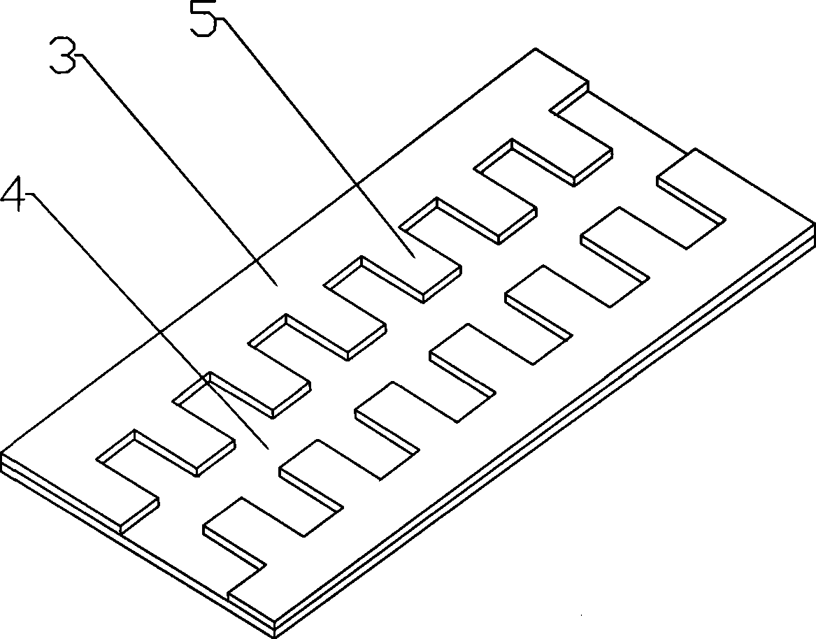
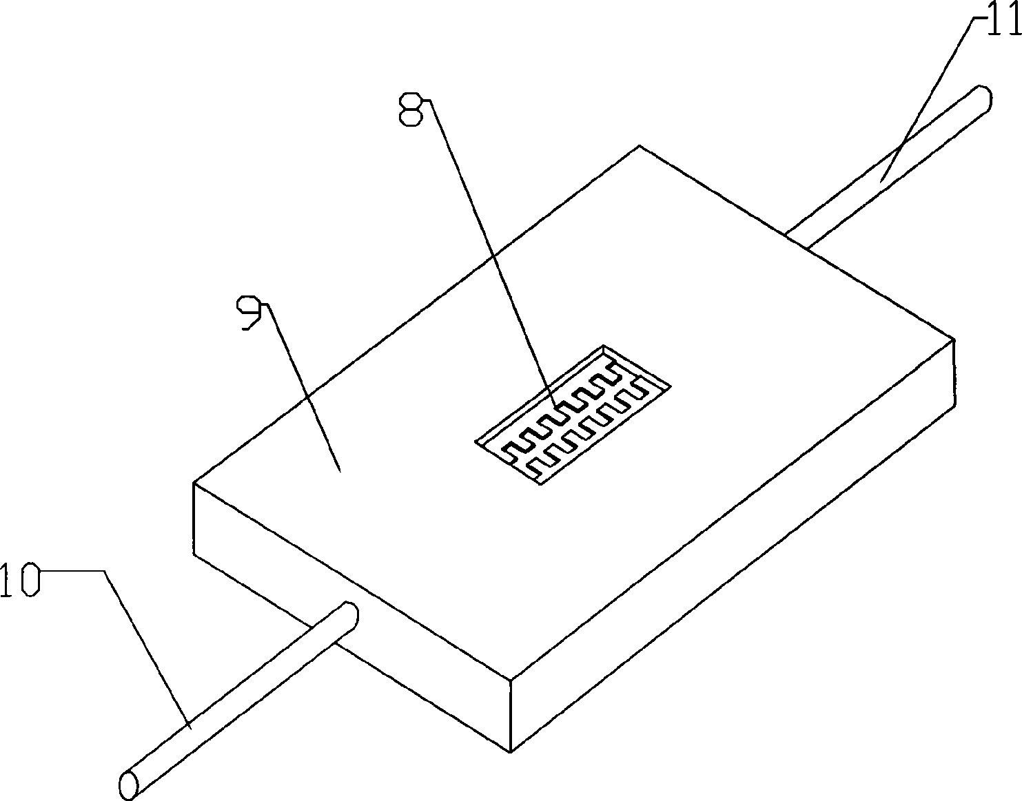
[0037] figure 1 It is a schematic structural diagram of a cell electrofusion chip; figure 1 As shown: the cell electrofusion chip is formed by bonding a silicon wafer 1 and a glass wafer 2, a microelectrode group 3 is arranged on the silicon wafer 1, and a plurality of microelectrodes 5 are arranged on the microelectrode group 3, and the microelectrode group 3 A signal lead-out line is provided to connect with an external electrical control signal. The microelectrodes 5 are arranged on one side of the microelectrode group 3 in a zigzag shape. A continuous microchannel 4; the thickness of the silicon chip 1 is 40-60 μm, and the thickness of the glass sheet 2 is 500-1000 μm; the signal lead-out line of the microelectrode 5 is made of gold wire.

[0038] The microelectrodes 5 can also be arranged on the microelectrode group 3 in a sharp-edged zigzag shape or other shapes.

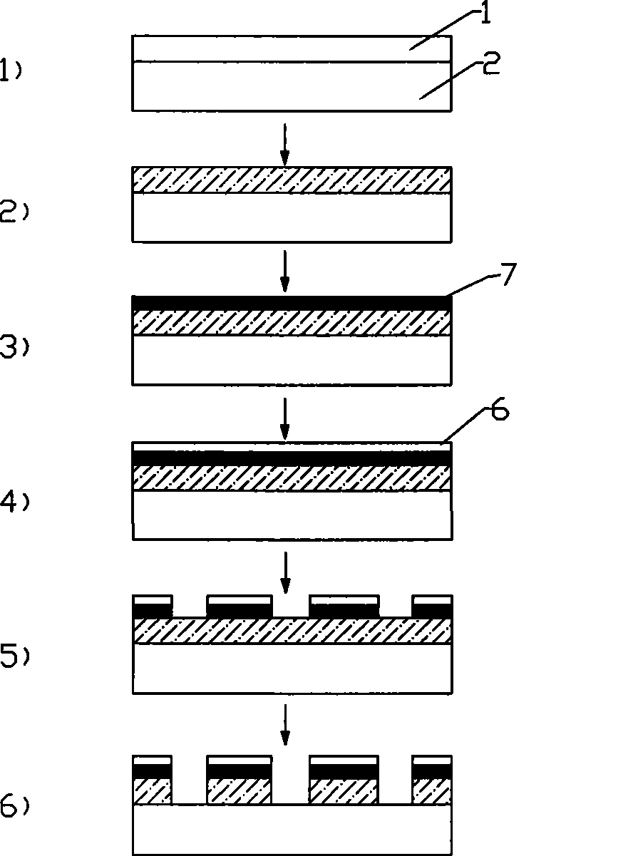
[0039] figure 2 Schematic diagram of the fabrication process for the cell electrofusion chip, such as ...


PUM

PropertyMeasurementUnit
thicknessaaaaaaaaaa
thicknessaaaaaaaaaa
thicknessaaaaaaaaaa

Abstract

The invention discloses a cell electrofusion chip which is formed by bonding a silicon wafer and a glass sheet, wherein microelectrode units are arranged on the silicon wafer, a plurality of microelectrodes are arranged on the microelectrode units, and the microelectrode units are provided with signal leading-out wires; the microelectrodes are arranged on one side or two sides of each microelectrode unit in a jagged shape, the microelectrodes arranged on the adjacent microelectrode units are opposite in a staggered way, and a continuous microchannel is formed among the microelectrode units; the cell electrofusion chip not only can observe and record the cell fusion process more easily during the fusion process, but also can improve the anti-chemical corrosion ability, the high-temperature and high-pressure resistant ability and the biocompatibility of the cell electrofusion chip; meanwhile, the invention also discloses a manufacturing method of the cell electrofusion chip.

Description

technical field [0001] The invention relates to the technical field of biological cell fusion, in particular to a cell electric fusion chip and a manufacturing method. Background technique [0002] Biological cells can form new cells through fusion, which is of great significance in the basic field of modern biomedical engineering. It is widely used in research fields such as medical care and modern agriculture, including the preparation of monoclonal antibodies, the generation or improvement of new species, etc. Cell fusion includes chemical fusion methods (such as PEG method) and physical fusion methods. Among the physical fusion methods, the electric field fusion method has been widely used because of its advantages of easy precise control, good repeatability, and high fusion rate. [0003] Cell electrofusion is achieved through several continuous processes: cells are subjected to dielectrophoretic force in an electric field, and they contact each other to form bead strin...

Claims


Application Information

Patent Timeline
Patent Type & Authority Applications(China)
IPC IPC(8): C12M1/42C12M3/00
CPCC12M35/02
Inventor 阴正勤曹毅杨军徐海伟郑小林胡宁夏斌杨静许蓉
Owner ARMY MEDICAL UNIV
Why Eureka
Try Eureka