Preparation method of planar magnetic core spiral structure micro-inductance device
A technology of helical structure and plane helix is applied in the field of preparation of micro-inductance devices, which can solve the problems of device performance impact, difficulty in obtaining high-performance micro-inductance devices, etc., achieve high operating frequency, avoid undercutting phenomenon, and improve high-frequency characteristics. Effect
- Summary
- Abstract
- Description
- Claims
- Application Information
AI Technical Summary
Problems solved by technology
Method used
Image

Examples
Embodiment 1
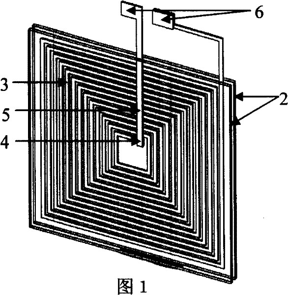
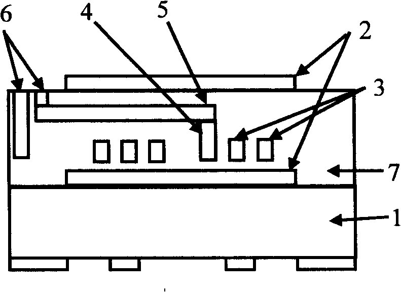
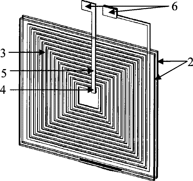
[0049] (1) Sputter a 30nm-thick Cr layer on one side of the cleaned glass substrate (referred to as the B side), throw the positive glue AZ4000 series, the thickness of the photoresist is 3 μm, and then dry the photoresist ; Expose and develop the photoresist on the back, etch the Cr layer in the etching solution, and then remove all the photoresist with acetone; throw polyimide to a thickness of 3 μm, and then perform polyimide drying and curing process , resulting in a double-sided overlay alignment symbol.
[0050] (2) Spray epoxy resin AB glue on the other side of the glass substrate (called A side), and then bond the magnetic core material on the A side of the substrate, and let it dry naturally. The following processes are all carried out on side A;
[0051] (3) Throw away the positive resist, the thickness of the photoresist is 5 μm, dry the photoresist; expose and develop; then etch the magnetic core material in the acid etching solution, remove the photoresist and ep...
Embodiment 2
[0067] (1) Sputter a 50nm-thick Cr layer on one side of the cleaned glass substrate (referred to as the B side), throw the positive glue AZ4000 series, the thickness of the photoresist is 4 μm, and then dry the photoresist ; Expose and develop the photoresist on the back, etch the Cr layer in the etching solution, and then remove all the photoresist with acetone; throw polyimide to a thickness of 4 μm, and then perform polyimide drying and curing process , resulting in a double-sided overlay alignment symbol.
[0068] (2) Spray epoxy resin AB glue on the other side of the glass substrate (called A side), and then bond the magnetic core material on the A side of the substrate, and let it dry naturally. The following processes are all carried out on side A;
[0069] (3) Throw away the positive resist, the thickness of the photoresist is 8 μm, dry the photoresist; expose and develop; then etch the magnetic core material in the acid etching solution, remove the photoresist and ep...
Embodiment 3
[0085] (1) Sputter a layer of 80nm thick Cr layer on one side of the cleaned glass substrate (referred to as the B side), throw the positive glue AZ4000 series, the thickness of the photoresist is 5 μm, and then dry the photoresist ; Expose and develop the photoresist on the back side, etch the Cr layer in the etching solution, and then remove all the photoresist with acetone; throw polyimide with a thickness of 5 μm, and then perform polyimide drying and curing process , resulting in a double-sided overlay alignment symbol.
[0086] (2) Spray epoxy resin AB glue on the other side of the glass substrate (called A side), and then bond the magnetic core material on the A side of the substrate, and let it dry naturally. The following processes are all carried out on side A;
[0087](3) Throw away the positive resist, the thickness of the photoresist is 10 μm, dry the photoresist; expose and develop; then etch the magnetic core material in the acid etching solution, remove the ph...
PUM
| Property | Measurement | Unit |
|---|---|---|
| thickness | aaaaa | aaaaa |
| thickness | aaaaa | aaaaa |
| width | aaaaa | aaaaa |
Abstract
Description
Claims
Application Information
 - R&D
- Intellectual Property
- Life Sciences
- Materials
- Tech Scout
- Unparalleled Data Quality
- Higher Quality Content
- 60% Fewer Hallucinations
Browse by: Latest US Patents, China's latest patents, Technical Efficacy Thesaurus, Application Domain, Technology Topic, Popular Technical Reports.
© 2025 PatSnap. All rights reserved.Legal|Privacy policy|Modern Slavery Act Transparency Statement|Sitemap|About US| Contact US: help@patsnap.com