Multi-junction solar cell with monocrystalline silicon substrate

A multi-junction solar cell and solar cell technology, which is applied in circuits, photovoltaic power generation, electrical components, etc., can solve problems such as the high price of gallium arsenide single wafers, restrictions on large-scale applications, and the impact on the cost of concentrating solar cells

Inactive Publication Date: 2009-07-15
北京索拉安吉清洁能源科技有限公司
View PDF0 Cites 26 Cited by
  • Summary
  • Abstract
  • Description
  • Claims
  • Application Information

AI Technical Summary

Problems solved by technology

[0004] However, germanium single wafers and gallium arsenide single wafers currently used as substrate materials for III-V compound semiconductor solar c

Method used


Image

  • Multi-junction solar cell with monocrystalline silicon substrate

Examples


Embodiment Construction

[0011] In order to further illustrate the structure and features of the present invention, the present invention will be further described below in conjunction with the embodiments and accompanying drawings.

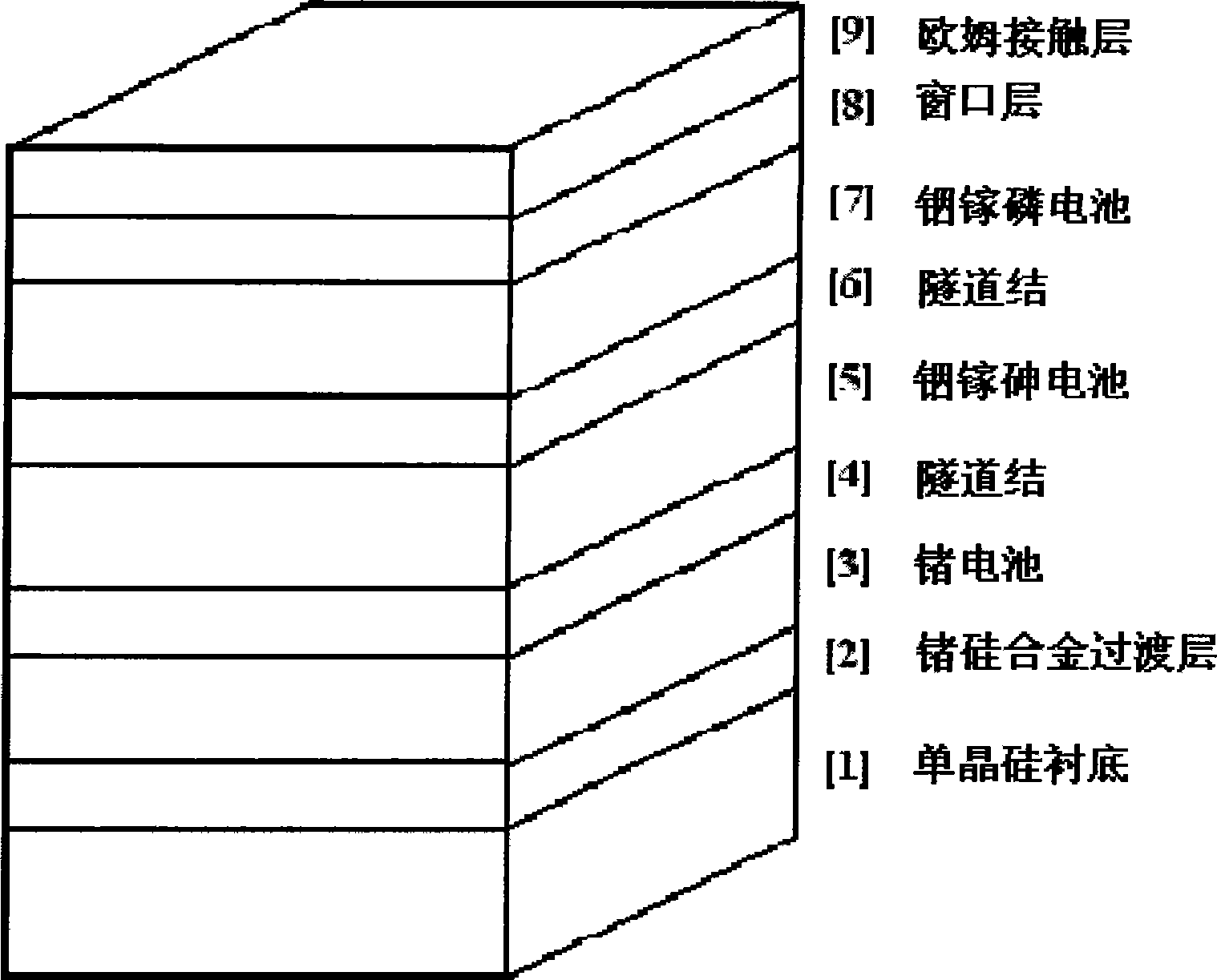
[0012] Such as figure 1 Shown, a method for preparing multi-junction solar cells based on single crystal silicon substrates. Using the metal-organic chemical vapor deposition (MOCVD) method, using a single crystal silicon wafer [1] as a substrate, first grow a germanium-silicon alloy transition layer [2], and then grow a germanium bottom cell [3] to connect the germanium bottom cell and indium Tunnel junction of GaAs intermediate cell[4], InGaAs intermediate cell[5], tunnel junction connecting InGaAs intermediate cell and InGaP top cell[6], InGaP top cell[7], window layer (n-AlGaP)[8] and ohmic contact layer (n + -GaAs)[9].

[0013] After growing a multi-junction solar cell wafer based on a single crystal silicon substrate, conventional photolithography, coating and s...


PUM


Abstract

The invention discloses a multi-junction solar cell based on a monocrystalline silicon substrate for the solar energy power generation, especially suitable for a high efficiency concentrated solar energy power generation system characterized by growing the multi-junction solar cell materials by using a silicon single-crystal wafer as a substrate through a Metal Organic Chemical Vapor Deposition (MOCVD) method or a Molecular Beam Epitaxy (MBE) method. Firstly a germanium-silicon alloy transition layer is grown on the silicon single-crystal wafer, then a germanium cell structure, an indium-gallium-arsenic cell structure and an indium-gallium-phosphorus cell structure are grown in turn. The invention employs the silicon single-crystal sheet instead of the germanium single-crystal wafer and the gallium arsenide single-crystal wafer, greatly reduces the multi-junction solar cell cost, improves the conversion efficiency of the silicon based solar cell and expedites the application and development of the solar energy power generation.

Description

technical field [0001] The invention provides a method for preparing a multi-junction solar cell based on a single crystal silicon substrate. Background technique [0002] Solar cells can use the interaction between sunlight and materials to directly generate electricity. It is one of the most eye-catching projects in the large-scale development and utilization of solar energy, and it is also the top priority for the sustainable development of energy. Among the many types of solar cells, the III-V compound semiconductor solar cells represented by GaAs have become one of the important fields of solar cell research and application due to their high conversion efficiency and good working stability. [0003] Due to the high material cost of III and V compound semiconductor solar cells, the price of cells is the most important part of the cost of photovoltaic systems, which restricts the application of III and V compound semiconductor solar cells. By adopting concentrating techn...

Claims


Application Information

Patent Timeline
IPC IPC(8): H01L31/042H01L31/052
CPCY02E10/52Y02E10/50
Inventor 索拉安吉
Owner 北京索拉安吉清洁能源科技有限公司
Why Eureka
Try Eureka