Germanium nanopoint/silicon nanowire array structure thin film and preparation thereof

A silicon nanowire array, silicon nanowire technology, applied in nanostructure manufacturing, nanotechnology, nanotechnology and other directions, can solve the problems of few layers of germanium nanodots, small diameter of germanium nanodots, low production cost, etc. Good, low cost of production equipment, high production efficiency

Active Publication Date: 2011-01-19
施毅
View PDF0 Cites 0 Cited by
  • Summary
  • Abstract
  • Description
  • Claims
  • Application Information

AI Technical Summary

Problems solved by technology

[0005] The main purpose of the present invention is in order to overcome above-mentioned existing adopting first epitaxial growth single-layer germanium nano-dot silicon and then on the basis of single-layer epitaxial growth multi-layer germanium nano-dot silicon thin film to exist germanium nano-dot layer number, light efficiency is not good For the disadvantages of high level, provide a germanium nano-dot / silicon nano-wire array structure with small diameter, many layers, the same crystal orientation, high electrical conductance in the axial direction, short growth time and low production cost film

Method used


Image

  • Germanium nanopoint/silicon nanowire array structure thin film and preparation thereof
  • Germanium nanopoint/silicon nanowire array structure thin film and preparation thereof
  • Germanium nanopoint/silicon nanowire array structure thin film and preparation thereof

Examples


Embodiment Construction

[0019] Preferred embodiments of the present invention are described in further detail below in conjunction with the accompanying drawings;

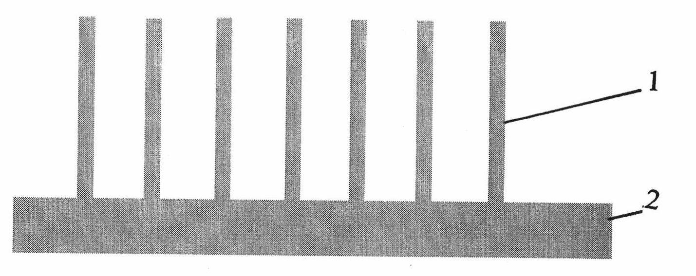
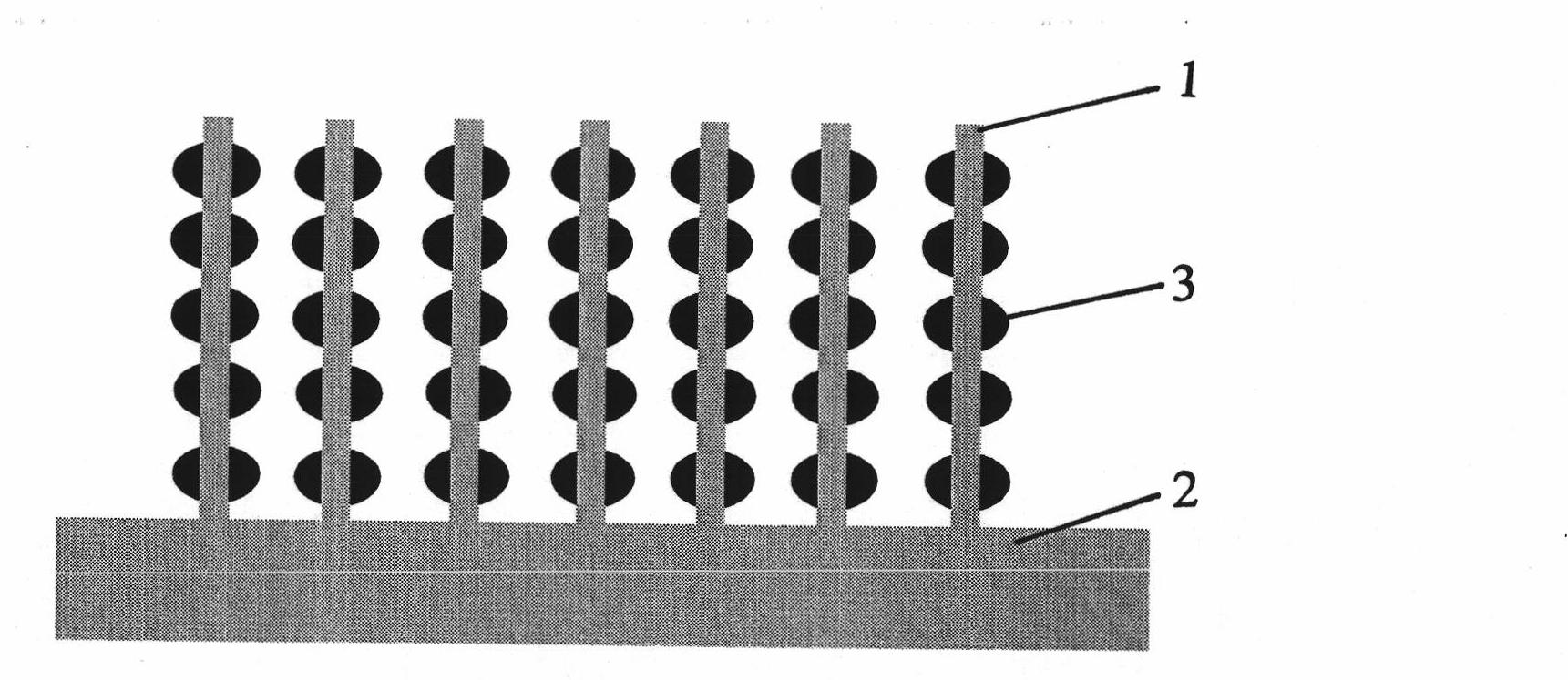
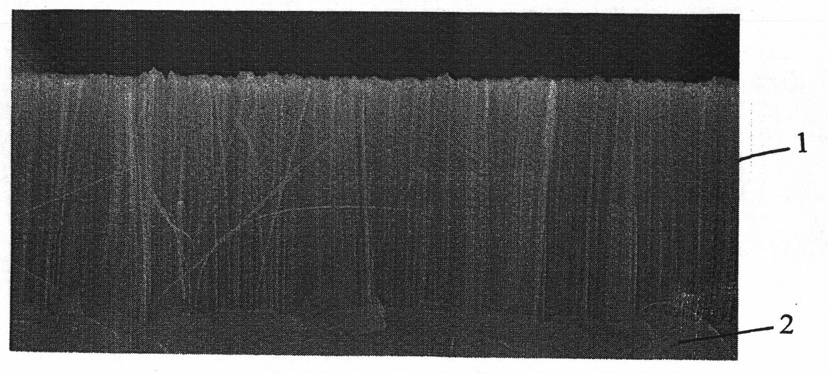
[0020] The germanium nano-dot / silicon nano-wire array structure thin film of the present invention is mainly composed of a silicon nano-wire array and germanium nano-dots, and the germanium nano-dots 3 are distributed on the silicon nano-wires 1 of the silicon nano-wire array.

[0021] Various techniques can be adopted for preparing the silicon nanowire array substrate in the present invention. For example, the method of utilizing chemical etching specifically includes: preparing a substrate, which can be a single crystal P-type silicon wafer, or a single crystal N-type silicon wafer, or a polycrystalline silicon wafer; After cleaning, silver is deposited on the surface of the substrate. The specific deposition method can be by evaporation, sputtering or chemical methods; substrate.

[0022] The solution etching method of the silicon na...


PUM

PropertyMeasurementUnit
lengthaaaaaaaaaa

Abstract

The invention provides a germanium nanometer point / silicon nanometer line array structural film, mainly consisting of silicon nanometer lines and germanium nanometer points distributed on the silicon nanometer lines of the silicon nanometer line array. The preparing method thereof mainly comprises steps as follows: with P or N type single crystal silicon and poly-silicon as raw materials, preparing large silicon nanometer line arrays by utilizing an etching method; and then applying low-pressure chemical vapor deposition technique and using germane as the gas source to prepare germanium points on substrates of the large silicon nanometer line arrays. With more layers of germanium nanometer points and high optical efficiency, the large-scale germanium nanometer point / silicon nanometer linearray structural film brings great benefits to the further production of high-efficiency optoelectronic devices. With the advantages of low cost of manufacturing equipment, high production efficiencyand greatly reduced cost and the like, the production method thereof is easy to be combined with the existing techniques of silicon film devices, and is considered as an optimized method for producing germanium nanometer point / silicon nanometer line array structural films.

Description

technical field [0001] The invention relates to a semiconductor low-dimensional structure film product and a preparation method thereof. More specifically, it relates to a thin film with a germanium (Ge) nano-dot / silicon (Si) nano-wire array mosaic structure and a preparation method thereof, belonging to the field of semiconductor devices. Background technique [0002] Due to the quantum confinement effect, the low-dimensional semiconductor structure has great changes in its electrical and optical properties. The three-dimensionally confined nanodot (Dots) structure is more attractive due to its strong quantum confinement effect on the carriers (such as electrons, holes, and excitons). Nanodot structure materials have extremely broad application prospects in optoelectronic devices and single electron devices. By controlling the shape, size and structure of nanodots, it is possible to effectively adjust the electronic behavior such as its energy gap width and exciton bindin...

Claims


Application Information

Patent Timeline
Patent Type & Authority Patents(China)
IPC IPC(8): B82B1/00B82B3/00
Inventor 叶敏华施毅濮林徐子敬张荣郑有炓
Owner 施毅
Why Eureka
Try Eureka