

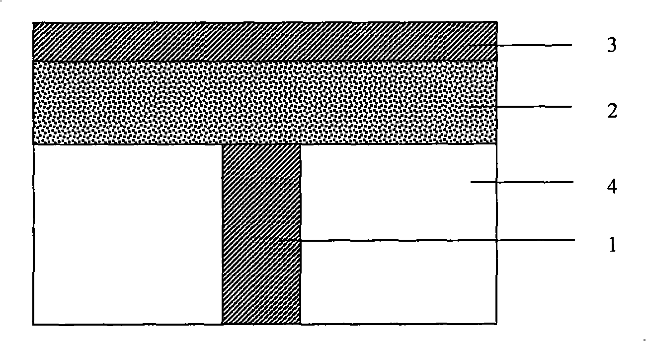
M-Sb-Se phase changing thin-film material used for phase changing memory
A phase-change memory and thin-film material technology, which is applied in the field of microelectronics, can solve the problems of phase-change memory application limitations, poor CMOS process compatibility, poor thermal stability, etc., and achieve good data retention characteristics, good compatibility, and fast crystallization speed. Effect
- Summary
- Abstract
- Description
- Claims
- Application Information
AI Technical Summary
Problems solved by technology
Method used
Image

Examples
Embodiment 1
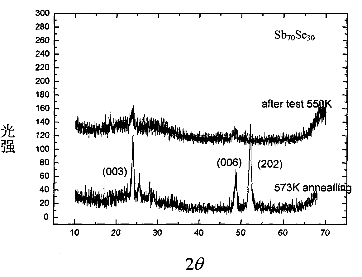
[0029] Figure 3a , Figure 3b , Figure 3c and Figure 3d is the composition of Sb 70 Se 30 , (Sb 70 Se 30 ) 96 W 4 , (Sb 70 Se 30 ) 90 W 10 , (Sb 70 Se 30 ) 80 W 20XRD test results of the W-Sb-Se thin film. The XRD spectrum shows that the W-Sb-Se film with the appropriate composition just prepared is in an amorphous state, without any diffraction peaks, and the high resistance state is an amorphous structure, while the XRD spectrum of the low resistance state W-Sb-Se film appears Sb The diffraction peaks of the W-Sb-Se films indicate that the phase transition occurs in the W-Sb-Se film, and the phase transition is closely related to Sb. see Figure 3a , the XRD pattern shows that for Sb 70 Se 30 When the material resistance drops to a certain level, Sb crystallizes when the film phase changes, indicating that the phase transition is related to Sb. see Figure 3b , in (Sb 70 Se 30 ) 96 W 4 The XRD pattern of the thin film material when the resistance...
Embodiment 2
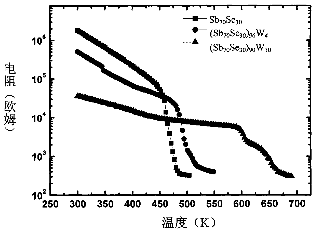
[0037] see Figure 6 , the shortest SET pulse of 20ns can crystallize the film, that is to say, the speed of the device from high resistance state to low resistance state is 20ns, which is much faster than that of Ge 2 Sb 2 Te 5 The SET speed of phase change memory is usually reported as 100ns~200ns.
[0038] The above embodiments are only used to illustrate rather than limit the technical solution of the present invention. Any modification or partial replacement that does not depart from the spirit and scope of the present invention shall fall within the scope of the claims of the present invention.
PUM
 Abstract
Description
Claims
Application Information