Low-temperature glass solder bonding and encapsulating method based on disc level glass micro-chamber

A technology of low-temperature glass solder and packaging method, which is applied in the direction of microstructure devices, coupling of optical waveguides, processing microstructure devices, etc., can solve the problems of poor packaging reliability, large thermal mismatch, and large limitations, and reduce the Package cost, low flatness requirements, and wide application range

Inactive Publication Date: 2011-09-14
SOUTHEAST UNIV
View PDF0 Cites 0 Cited by
  • Summary
  • Abstract
  • Description
  • Claims
  • Application Information

AI Technical Summary

Problems solved by technology

[0005] If a Pyrex7740 glass substrate containing a glass microcavity is used, and anodic bonding is used to perform wafer-level packaging of the device, the process requires high flatness of the bonding surface, and the MEMS device substrate that generally adopts surface micromachining technology cannot meet the requirements.
Moreover, because the process introduces a bonding voltage of more than 400V, it is easy to cause irreversible damage to the movable parts of the micro-nano size of MEMS
[0006] Nowadays, using metal solder bonding or polymer bonding technology, most of them use a whole piece of silicon substrate without microcavity structure or Pyrex7740 glass substrate to bond with the substrate wafer containing the device, only supported by the bonding solder layer The height of the packaging space is very limited, and the height is only about 1-6 μm, which is very easy to damage the devices on the substrate.
Moreover, the bonding solder layer and the silicon substrate tend to have a large thermal mismatch, which is prone to failure, so that the hermetic package fails, and its package reliability is very poor.

Method used


Image

  • Low-temperature glass solder bonding and encapsulating method based on disc level glass micro-chamber
  • Low-temperature glass solder bonding and encapsulating method based on disc level glass micro-chamber
  • Low-temperature glass solder bonding and encapsulating method based on disc level glass micro-chamber

Examples


Embodiment 1

[0026] A low-temperature glass solder bonding packaging method based on wafer-level glass microcavities, comprising the following steps:

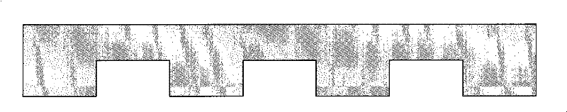
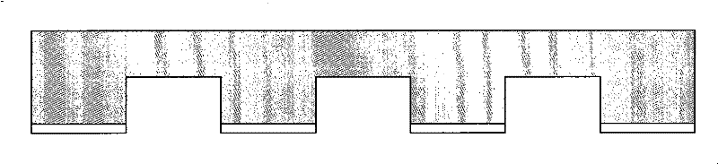
[0027] The first step is to use the screen printing process. The screen printing technology can use precision screen printing technology to coat the low-temperature glass solder on the package contact part of the Pyrex7740 glass substrate with a microcavity structure, and then apply the low-temperature glass solder Pre-baking, the pre-baking temperature is 350 ℃ ~ 450 ℃, usually slightly higher than the glass temperature of low temperature glass solder. The low-temperature glass solder is solidified and attached to the above-mentioned Pyrex7740 glass substrate with a microcavity structure. The low-temperature glass solder used here has a glass transition temperature of 330-500°C, such as 360°C, 375°C, 400°C, 430°C, At 470°C, the coefficient of thermal expansion is (20~50)×10 -7 / K glass solder (corresponding to the thermal expansion coeffi...

Embodiment 2

[0032]A low-temperature glass solder bonding packaging method based on a wafer-level glass microcavity, the steps of the packaging method are the same as in Example 1, but the glass microcavity is prepared by the following method:

[0033] In this embodiment, the preparation method of the microcavity structure on the Pyrex7740 glass substrate is as follows: the first step is to use silicon micromachining technology to manufacture a glass microcavity pattern structure on a double-sided polished silicon wafer; The wafer and the Pyrex7740 glass wafer of the same size are bonded under a pressure of less than 1Pa, so that the glass microcavity pattern structure is sealed into a vacuum cavity. The third step is to heat the above-mentioned bonded wafer under an atmospheric pressure to 810°C-890°C, such as 830°C, 850°C, 870°C, keep warm for 3-5 minutes, the time can be selected as 4 minutes, the pressure difference between the inside and outside of the cavity makes the softened glass f...

Embodiment 3

[0035] A method for low-temperature glass solder bonding packaging of a novel wafer-level glass microcavity, comprising the following steps:

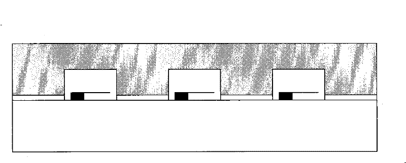
[0036] In the first step, the low-temperature glass solder is coated on the bonding contact part of the Pyrex7740 glass substrate with a microcavity structure by using a screen printing process.

[0037] In the second step, pre-baking is carried out near the glass transition temperature Tg of the low-temperature glass solder to volatilize the organic solvent in the solder and at the same time make the solder adhere tightly to the glass substrate.

[0038] The third step is to align the Pyrex7740 glass packaging wafer coated and cured with low-temperature glass solder with the silicon substrate containing CMOS circuits or MEMS devices, so that the microcavity structure is facing the packaged part on the substrate.

[0039] The fourth step is to complete the alignment of the two bonded sheets, which are clamped by the fixture to apply pre...


PUM

PropertyMeasurementUnit
heightaaaaaaaaaa
glass transition temperatureaaaaaaaaaa

Abstract

The invention discloses a low-temperature glass solder bonding and packaging method based on wafer-level glass microcavities, which comprises the following steps: firstly, utilizing a silk-screen printing process to coat low-temperature glass solder on a packaging contact part of a Pyrex7740 glass substrate provided with a microcavity structure, preliminarily drying the low-temperature glass solder, and making the low-temperature glass solder be cured and cling to the Pyrex7740 glass substrate provided with the microcavity structure; secondly, aligning a Pyrex7740 glass packaging wafer which is cured with the low-temperature glass solder and a silicon substrate wafer comprising an MEMS device or a CMOS circuit, and making the microcavity structure on the Pyrex7740 glass substrate correspond to the position of the MEMS device or the CMOS circuit to be packaged of a silicon substrate; and thirdly, using a clamper to firmly clamp the two aligned wafers, applying the pressure, sintering the glass solder in a specified packaging atmosphere, and cooling the glass solder. The whole process is based on integral processing of the silicon wafer and the Pyrex7740 glass wafer, belongs to a process for manufacturing and packaging a wafer-level MEMS, and has the characteristics of simple method, adjustable packaging space and low cost.

Description

technical field [0001] The invention relates to a MEMS (micro-electro-mechanical system) manufacturing and packaging technology, in particular to a low-temperature glass solder bonding packaging method based on a wafer-level glass microcavity. Background technique [0002] In the field of MEMS manufacturing technology, Pyrex7740 glass (a kind of glass containing alkaline ions, Pyrex is the product brand of Corning Company) is an important material, it has the same semiconductor silicon material (at room temperature 300K, the thermal expansion coefficient of Pyrex7740 glass is 28 ×10 -7 / K, the thermal expansion coefficient of silicon is 23~40×10 -7 / K) similar thermal expansion coefficient, high light transmittance and high strength, can be used for high-strength anodic bonding with silicon, and can also be integrated with silicon substrates by metal solder bonding or polymer bonding. chip bonding. Due to such characteristics, Pyrex7740 glass is widely used in MEMS packag...

Claims


Application Information

Patent Timeline
Patent Type & Authority Patents(China)
IPC IPC(8): H01L21/56B81C3/00B81B7/02
Inventor 黄庆安柳俊文尚金堂唐洁影
Owner SOUTHEAST UNIV
Why Eureka
Try Eureka