

Flexible and wholly transparent ZnMgO thin film transistor and manufacturing method thereof
A thin-film transistor, transparent technology, applied in transistors, semiconductor/solid-state device manufacturing, semiconductor devices, etc., can solve the problems of pixel aperture ratio not reaching 100%, complex process, strong photosensitivity, etc., to achieve rich raw materials, simple process, good transparency
- Summary
- Abstract
- Description
- Claims
- Application Information
AI Technical Summary
Problems solved by technology
Method used
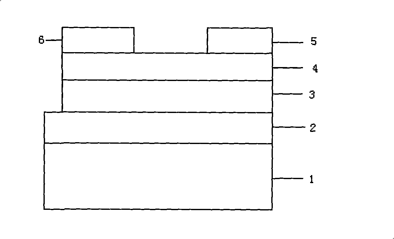
Image

Examples
Embodiment 1
[0024] The flexible fully transparent ZnMgO thin film transistor is prepared by magnetron sputtering technology, and the specific steps are as follows:
[0025] 1) Weigh ZnO and Ga with a purity greater than 99.99% 2 o 3 Powder, wherein the molar percentage of Ga is 4%. The weighed ZnO and Ga 2 o 3 The powder is poured into a ball mill jar with agate balls, and milled on a ball mill for 24 hours, the purpose is to make the powder mix evenly and refine it to a certain extent. Then the raw materials are separated and dried, added with a binder for grinding, and pressed into shape. Put the formed green body into the sintering furnace, discharge elements at low temperature (400°C) to volatilize the binder, and then raise the temperature to 1200°C for 4 hours to obtain a Ga-doped ZnO ceramic target.
[0026] 2) According to the chemical formula Zn 1-x Mg x O Weigh ZnO and MgO powders with a purity greater than 99.99%, x = 0.2, pour the weighed ZnO and MgO powders into a ball...
Embodiment 2
[0033] The preparation steps are the same as in Example 1, but the difference is that Zn 1-x Mg x The Mg content in the O thin film is x=0.3. The thin film transistor device is an n-channel enhancement type with a field effect mobility of 12cm 2 / Vs, the transmittance of the device in the visible region is higher than 80%, the device can be bent by 120° and the performance remains stable.
PUM
| Property | Measurement | Unit |
|---|---|---|
| transmittivity | aaaaa | aaaaa |
Abstract
Description
Claims
Application Information