Device and method for preparing optical waveguide in transparent solid material by femtosecond laser
A technology of femtosecond laser and transparent solid, which is applied in the manufacture of two-dimensional or three-dimensional optical waveguides and devices. In the field of devices for manufacturing optical waveguides in transparent solid materials, femtosecond lasers can solve problems such as complex processes and inability to manufacture three-dimensional waveguides. , to achieve the effect of convenient production
- Summary
- Abstract
- Description
- Claims
- Application Information
AI Technical Summary
Problems solved by technology
Method used
Image

Examples
Embodiment 1
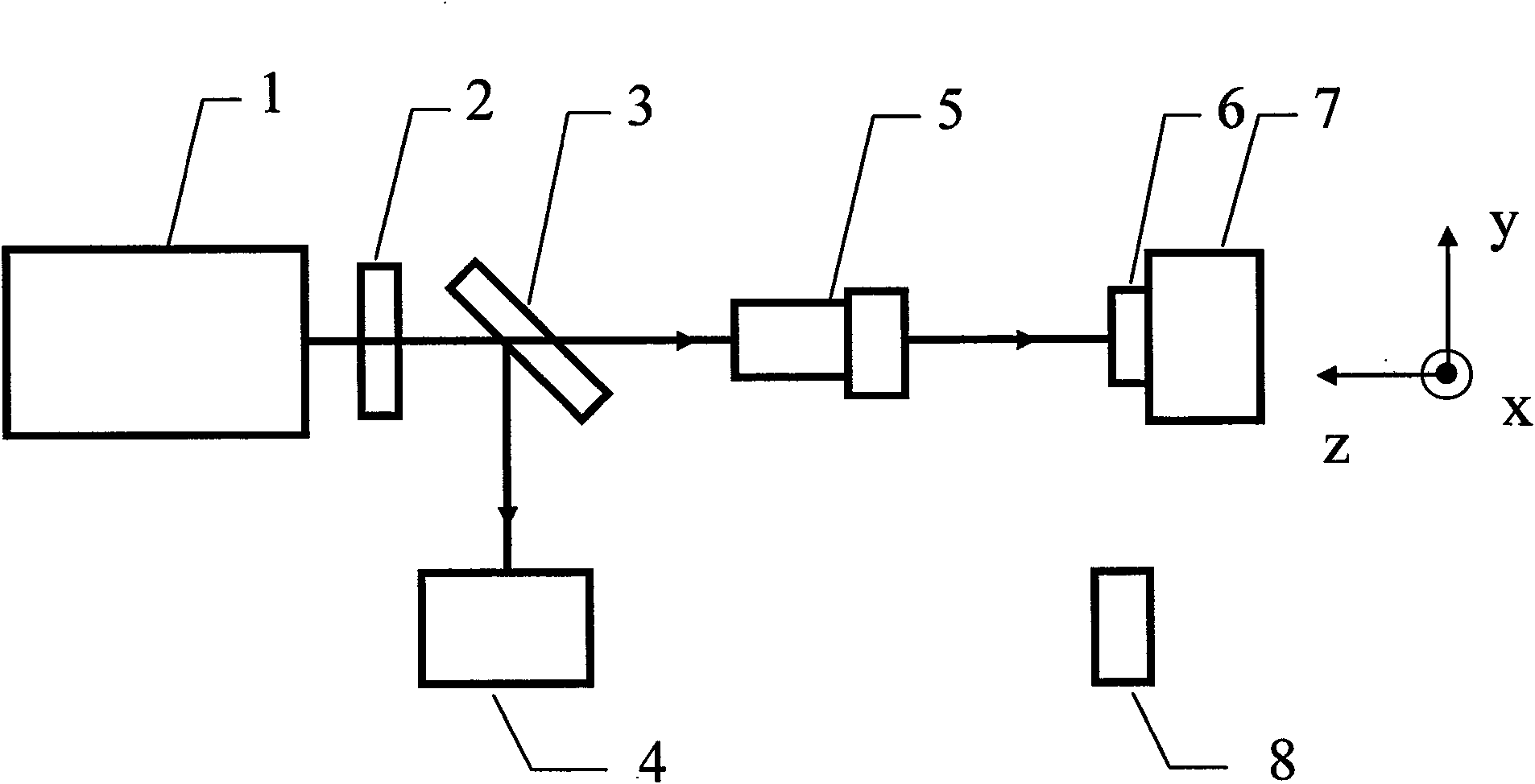
[0037] Embodiment 1, the manufacturing device of optical waveguide
[0038] like figure 1 As shown, the production device includes in turn:
[0039] Femtosecond laser system 1: used to provide femtosecond laser pulses for writing optical waveguides;
[0040] Variable attenuator 2: According to the needs of optical waveguide writing, it is used to attenuate the high-energy femtosecond laser pulse output by the femtosecond laser;
[0041] Beam splitter 3: used to split the femtosecond laser pulse attenuated by the variable attenuator;
[0042] Power meter 4: After the femtosecond laser beam is split by the beam splitter, one of the beams is coupled into the power meter to monitor the energy of the femtosecond laser pulse for writing;
[0043]High numerical aperture microscopic objective lens 5: set on the main optical path of the femtosecond laser pulse behind the beam splitter, used to tightly focus the femtosecond laser pulse, and the focused femtosecond pulse is vertically...
Embodiment 2
[0046] Embodiment 2, the manufacture of three-dimensional 1 × 3 optical beam splitter
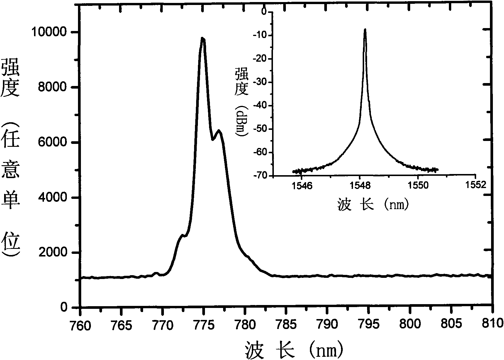
[0047] A femtosecond laser beam with a center wavelength of 800nm, a pulse width of 50fs, and a repetition rate of 1kHz was used as the writing laser beam, which was tightly focused into the fused silica glass for writing to produce a three-dimensional beam splitter.
[0048] The femtosecond laser 1 produces a femtosecond laser with a central wavelength of 800nm, a pulse width of 50fs, and a repetition rate of 1kHz. The pulse energy can generally reach the order of mJ. The variable attenuator 2 is used to attenuate the femtosecond pulse energy to about 0.5μJ. The beam splitter 3 splits the femtosecond laser beam, and the power meter 4 monitors the energy of the pulse, so that the variable attenuator 2 can be used to adjust the pulse energy to the required energy level accurately and timely. The femtosecond laser beam with adjusted energy is tightly focused by the microscopic objective lens ...
Embodiment 3
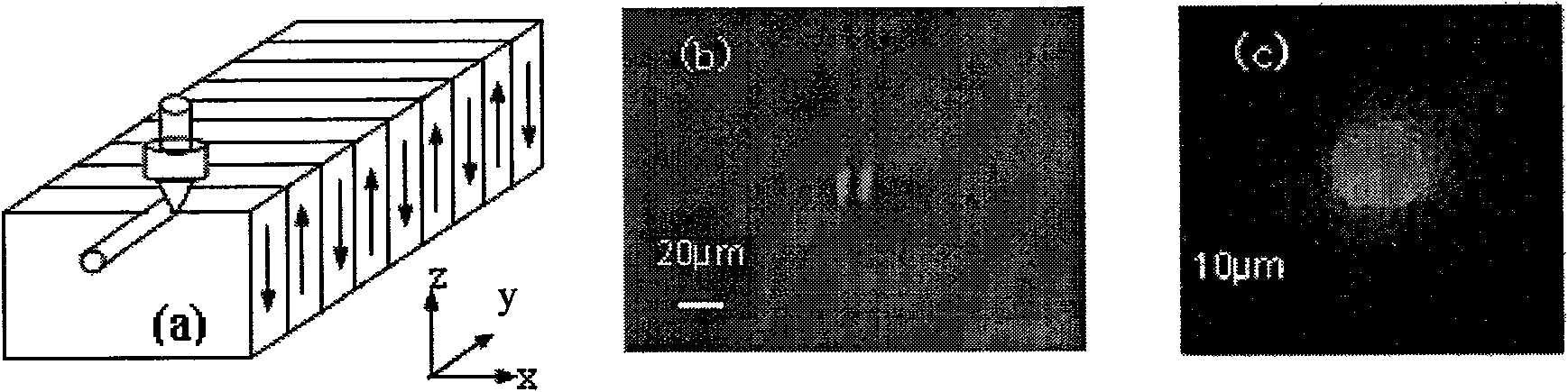
[0049] Embodiment 3, the making of two-dimensional Y-shaped beam splitter
[0050] A femtosecond laser with a center wavelength of 775nm, a pulse width of 150fs, and a repetition rate of 1kHz is used as the writing laser beam, and it is tightly focused into a z-cut lithium niobate (LN) crystal to write a buried optical waveguide and produce a two-dimensional Y-type beam splitter.
[0051] The femtosecond laser 1 produces a femtosecond laser with a center wavelength of 775nm, a pulse width of 150fs, and a repetition rate of 1kHz. The pulse energy can reach 0.5mJ. The femtosecond pulse energy is attenuated to about 10μJ by the variable attenuator 2, and the beam splitter is used to 3. The femtosecond laser beam is split, and the power meter 4 monitors the energy of the pulse, so that the variable attenuator 2 can be used to adjust the pulse energy to the required energy level accurately and timely. The femtosecond laser beam with adjusted energy is tightly focused by the micros...
PUM
| Property | Measurement | Unit |
|---|---|---|
| Center wavelength | aaaaa | aaaaa |
| Pulse width | aaaaa | aaaaa |
Abstract
Description
Claims
Application Information
 - R&D
- Intellectual Property
- Life Sciences
- Materials
- Tech Scout
- Unparalleled Data Quality
- Higher Quality Content
- 60% Fewer Hallucinations
Browse by: Latest US Patents, China's latest patents, Technical Efficacy Thesaurus, Application Domain, Technology Topic, Popular Technical Reports.
© 2025 PatSnap. All rights reserved.Legal|Privacy policy|Modern Slavery Act Transparency Statement|Sitemap|About US| Contact US: help@patsnap.com