

Silicon cantilever sensor, preparation method and application thereof
A cantilever beam and sensor technology, applied in the field of micro-nano sensors
- Summary
- Abstract
- Description
- Claims
- Application Information
AI Technical Summary
Problems solved by technology
Method used
Image

Examples
Embodiment 1
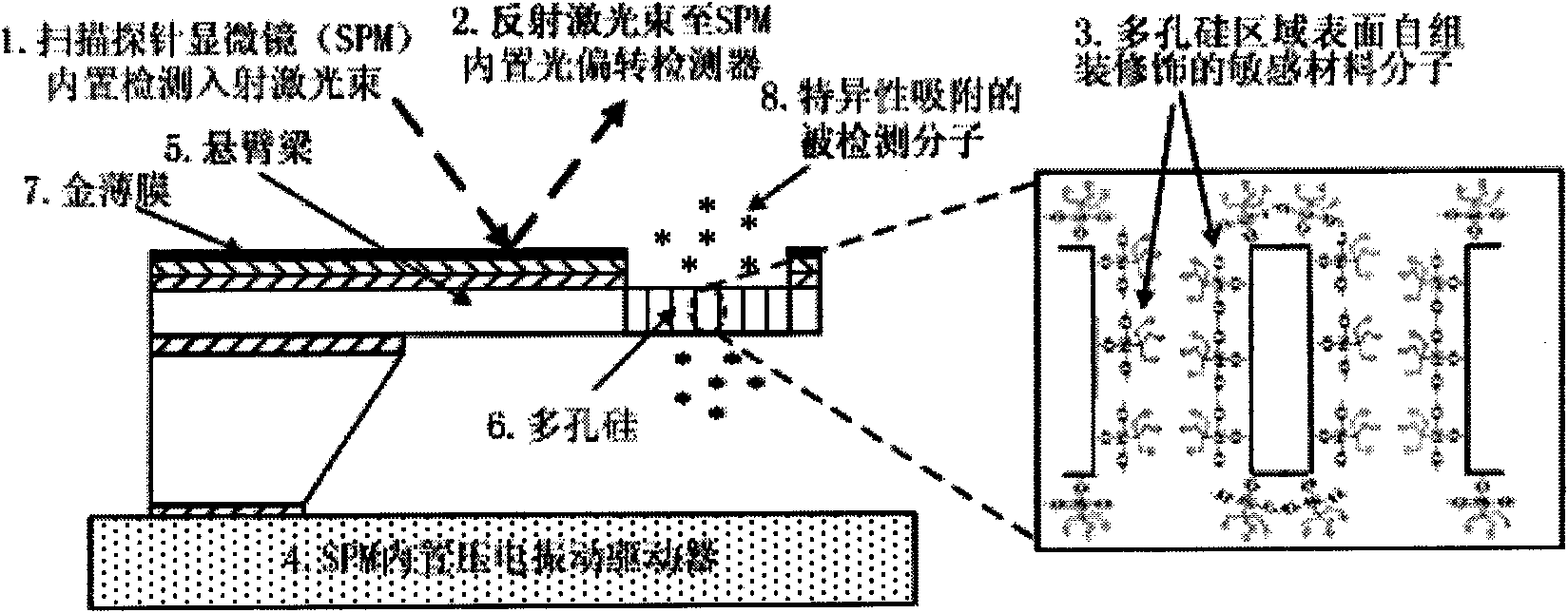
[0046] Explosive trinitrotoluene (TNT) chemical gas sensor
[0047] This implementation application takes the detection of explosive trinitrotoluene (TNT) gas as an example to describe the application of the present invention in chemical gas detection in detail.
[0048] Explosives Trinitrotoluene (TNT) is a commonly used explosive and is therefore an extremely hazardous hazard. Effective detection of TNT volatile gas will provide technical support for security checks and anti-terrorism in transportation hubs and important locations such as airports, stations, ports, and customs, and is of great significance to ensuring public safety.
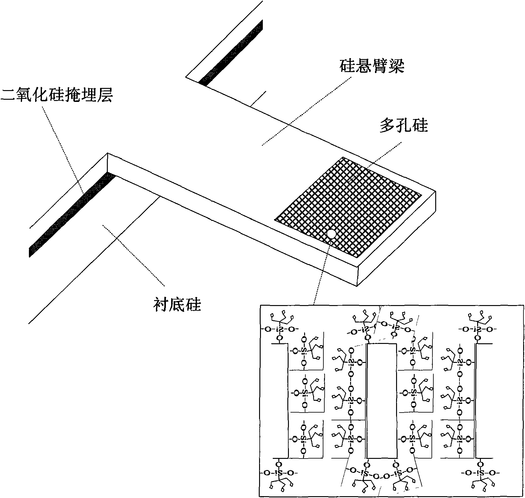
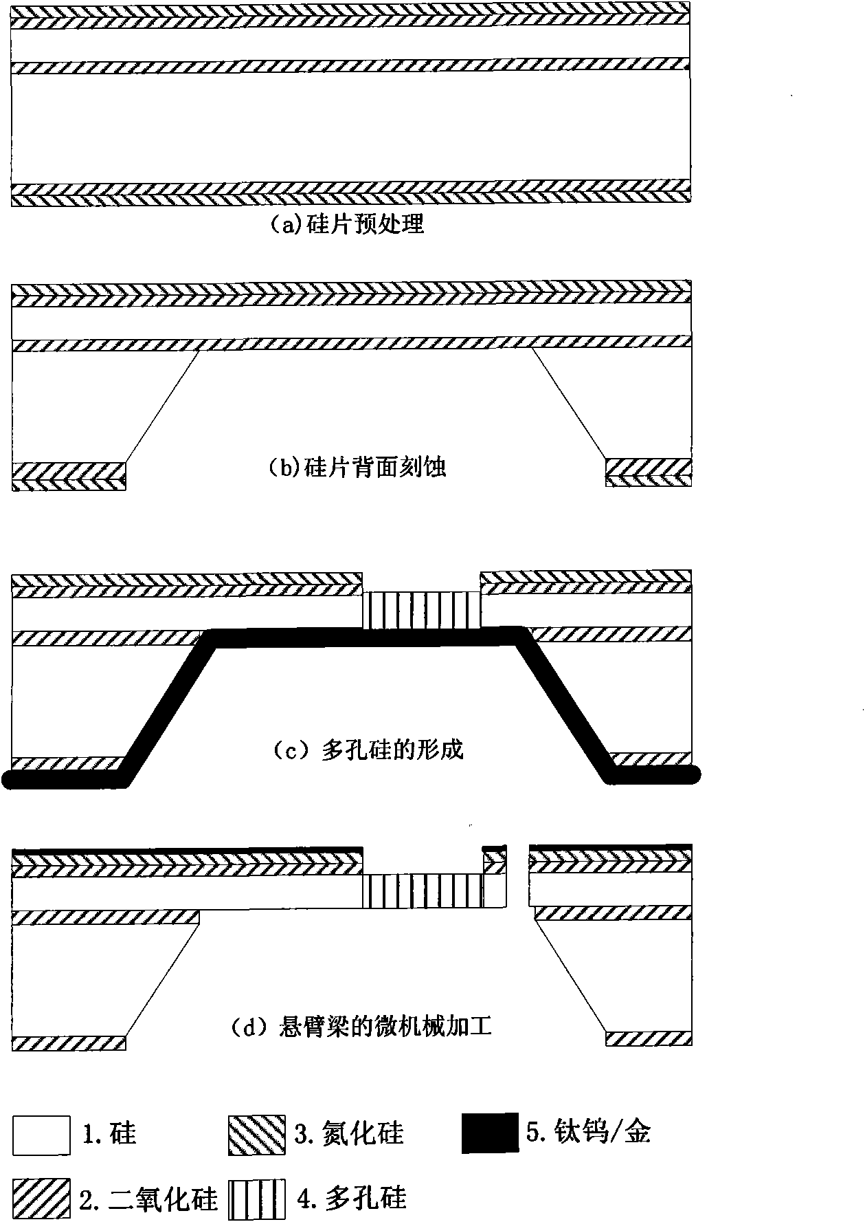
[0049] Fabrication of a 300μm×100μm×3μm porous silicon cantilever beam sensor, see attached figure 2 , the first resonance frequency of its bending mode is around 100kHz, and its specific preparation steps are as follows:
[0050] (a), wafer pretreatment
[0051] A double-sided polished SOI silicon wafer with n-type doped (100) crystal plan...
PUM
| Property | Measurement | Unit |
|---|---|---|
| Aperture | aaaaa | aaaaa |
| Resistivity | aaaaa | aaaaa |
| Thickness | aaaaa | aaaaa |
Abstract
Description
Claims
Application Information