Method for preparing thin film transistor

A thin-film transistor and thin-film technology, which is used in semiconductor/solid-state device manufacturing, electrical components, circuits, etc., can solve the problems of difficult to use flexible substrates, high gas purity requirements, and high costs, and achieves reduced preparation temperature, simple preparation process, and high cost. Effects of high mobility and on/off ratio

Inactive Publication Date: 2009-12-09
FUDAN UNIV
View PDF0 Cites 17 Cited by
  • Summary
  • Abstract
  • Description
  • Claims
  • Application Information

AI Technical Summary

Problems solved by technology

However, the PECVD method requires large equipment investment, high cost, high requirements on the purity of the gas, and is not easy to use on flexible substrates.

Method used


Image

  • Method for preparing thin film transistor
  • Method for preparing thin film transistor
  • Method for preparing thin film transistor

Examples


specific Embodiment approach

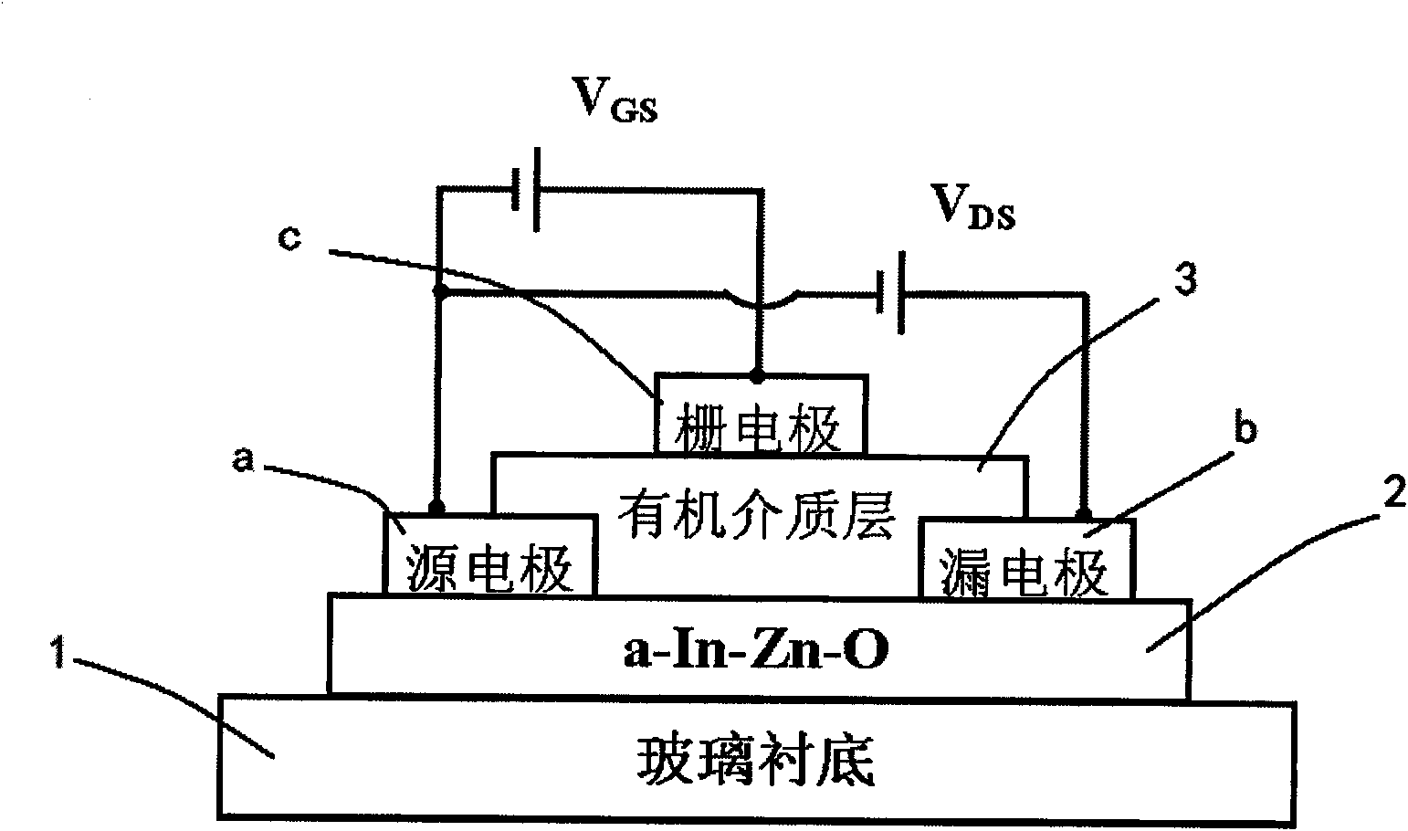
[0019] figure 1 Shown is the structure of a transparent amorphous oxide semiconductor thin film transistor with an organic dielectric layer according to the present invention, and 1 is a base layer, as shown in the figure is a glass substrate. At room temperature, a channel layer 2 is deposited on the base layer 1 by magnetron sputtering, which is composed of a transparent amorphous oxide film (a-In-Zn-O), and is used to connect the The source electrode a and the drain electrode b; then, an insulating organic dielectric layer 3 is covered on the channel layer 2 containing the source electrode a and the drain electrode b; finally, a gate electrode c is formed on the insulating layer 3.

[0020] According to the principle of the present invention, in order to obtain good carrier transfer performance of amorphous transparent oxide, indium zinc alloy or indium zinc oxide is used as the target material, wherein the atomic ratio of In and Zn varies in the range of 0.5-5.0, Use mature ...

Embodiment 1

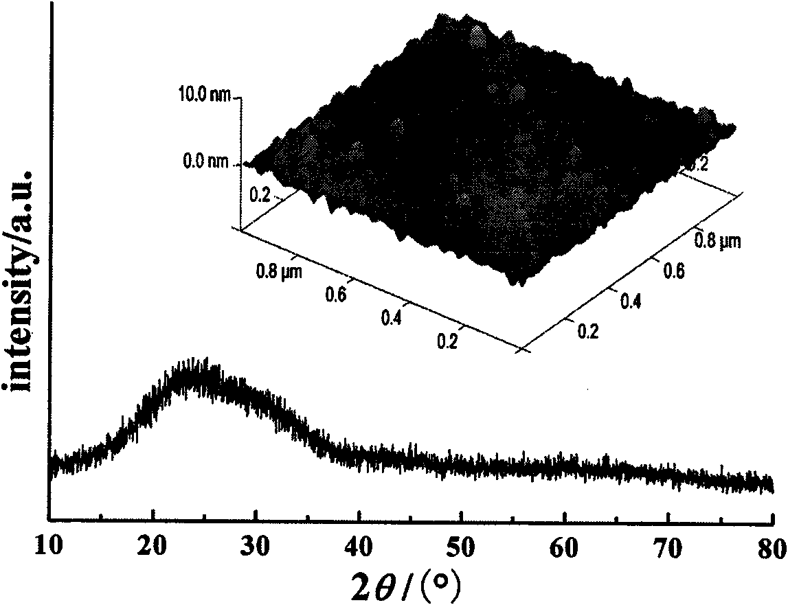
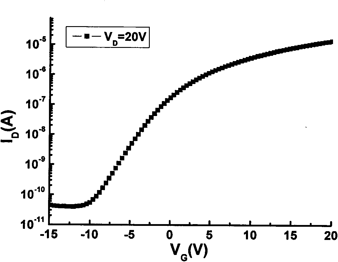
[0028] Use indium zinc alloy target (In:Zn=0.586:1 atomic ratio), and vacuum the reaction chamber to less than 2×10 before film deposition -3 Pa, and then O 2 And Ar gas are passed into the reaction chamber in turn, and the oxygen partial pressure in the reaction chamber is controlled to 5.0×10 -2 Pa, working pressure is 3.0×10 -1 Pa. The sputtering current and the sputtering voltage were adjusted to 120mA and 300V, respectively, and the sputtering time was 10 minutes to form a thin film on a common glass plate. The film thickness is about 110nm, and the resistivity is greater than 1×10 4 Ω·cm, the average transmittance of visible light is greater than 82%.

[0029] Using aluminum oxide masks with aspect ratios of 500 μm / 100 μm and 400 μm / 40 μm to prepare 80 nm aluminum films as source and drain electrodes by thermal evaporation, the thermal evaporation current is 50A, and the thermal evaporation voltage is 75V.

[0030] After 30 mg / mL of the PVP alcohol solution was mixed with ma...


PUM

PropertyMeasurementUnit
thicknessaaaaaaaaaa
electrical resistivityaaaaaaaaaa
transmittivityaaaaaaaaaa

Abstract

The invention belongs to the technical field of thin film transistors, and relates to a method for preparing a thin film transistor. The method comprises the following steps: by adopting indium-zinc alloy or indium-zinc oxide as a target material, under the room temperature, growing an indium-zinc oxide semiconductor thin film with a transparent amorphous structure on a substrate through magnetron sputtering technology, and forming a channel layer of the thin film transistor; preparing a source electrode and a drain electrode by adopting a thermal evaporation method; covering a layer of organic medium layer thin film manufactured by polyvinylpyrrolidone organic solution on the source electrode and the drain electrode by adopting a hauling or spinning method; and preparing a gate electrode on the organic medium layer thin film by adopting the thermal evaporation method. The atomic ratio of In to Zn in the target material is 0.5 to 5.0. The method can prepare a novel transparent thin film transistor with good electronic optical performance, has low preparation temperature and simple process, is favorable for large-area production, and has wide application prospect.

Description

Technical field [0001] The invention belongs to the technical field of thin film transistors, and specifically relates to a method for preparing a thin film transistor composed of a polyvinylpyrrolidone organic dielectric layer and an amorphous indium zinc oxide semiconductor channel layer. Background technique [0002] Thin Film Transistor (TFT) is a field effect transistor (Field Effect Transistor: FET), which is widely used in technical fields such as flat panel displays (FPD) due to its low turn-on voltage and high on / off current ratio. Its characteristic is to prepare tens of millions of TFT arrays with a size of several microns on a substrate several meters long diagonally to form a "large microelectronic" device. [0003] At present, the most widely used in active matrix liquid crystal display (AMLCD) is amorphous silicon transistor (a-Si TFT). However, because the carrier mobility of a-Si TFT is generally less than 1cm2 / V·s, it cannot meet the needs of fast response, high...

Claims


Application Information

Patent Timeline
Patent Type & Authority Applications(China)
IPC IPC(8): H01L21/34H01L21/363
Inventor 李桂锋张群周俊
Owner FUDAN UNIV
Why Eureka
Try Eureka